
Semiconductor package having multiple row of leads

a semiconductor and lead frame technology, applied in the direction of electrical apparatus construction details, casings/cabinets/drawers, electrical apparatus details, etc., can solve the problems of increased manufacturing costs, difficult individualization process (as a post-packaging process), and damage to the coherence of the bonding surface between the molding material and the lead frame, so as to achieve reliable semiconductor packages, reduce manufacturing costs, and enhance the planarity of leads

Active Publication Date: 2007-02-06
HAESUNG CO LTD
View PDF9 Cites 15 Cited by
  • Summary
  • Abstract
  • Description
  • Claims
  • Application Information

AI Technical Summary

Benefits of technology

This approach streamlines the post-packaging process, reduces manufacturing costs, enhances lead planarity, and prevents electrical shorts, enabling the production of semiconductor packages with more than two rows of leads effectively.

Problems solved by technology

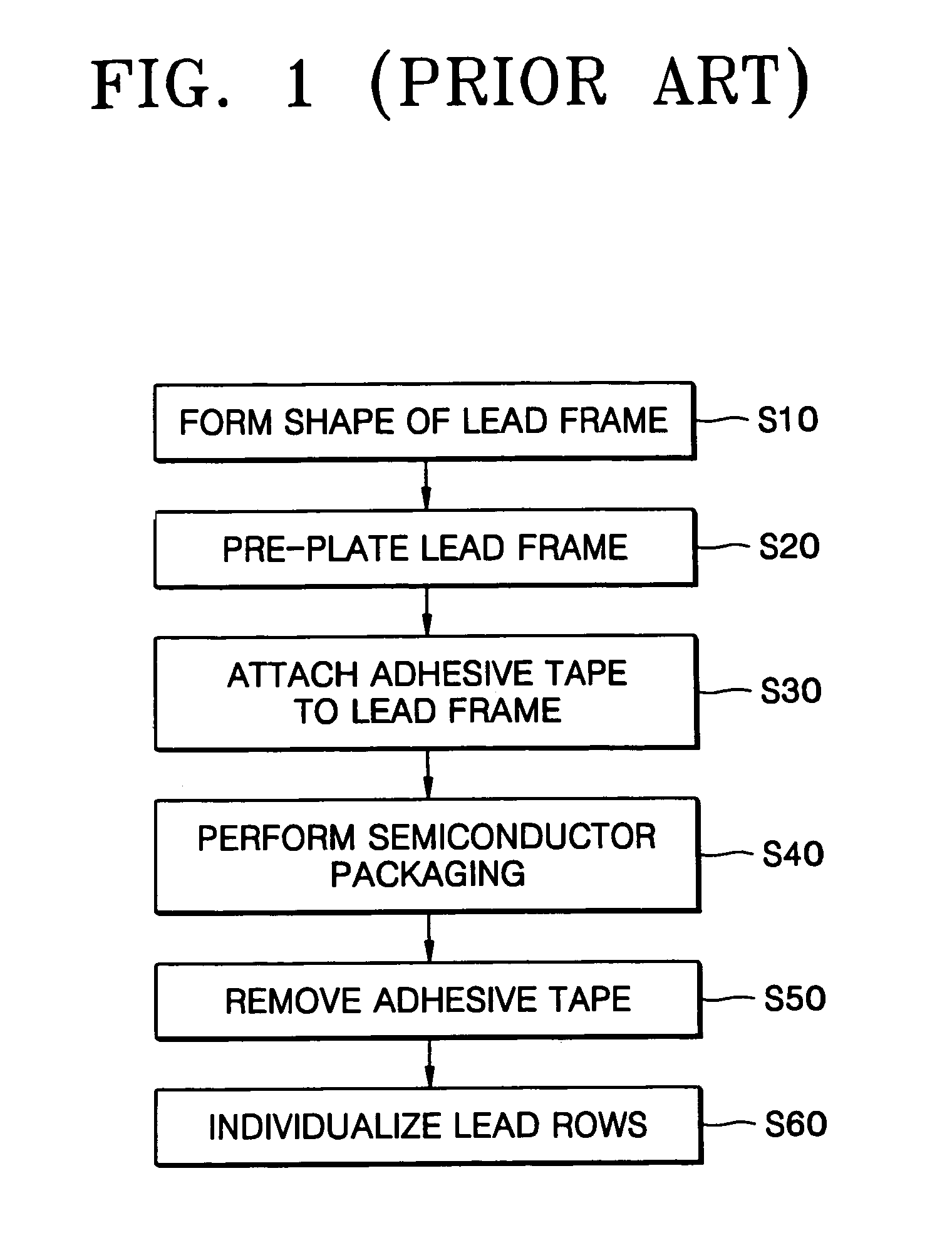
This individualization process (as a post packaging process) is difficult to perform and requires additional manufacturing costs.
In addition, coherence in the bonding surfaces between the molding material and the lead frame may be damaged because this process is performed as a post molding process.

Method used


Image

  • Semiconductor package having multiple row of leads
  • Semiconductor package having multiple row of leads
  • Semiconductor package having multiple row of leads

Examples


Embodiment Construction

[0025]Hereinafter, the present invention is described more in details with reference to the accompanying drawings, in which exemplary embodiments of the invention are shown.

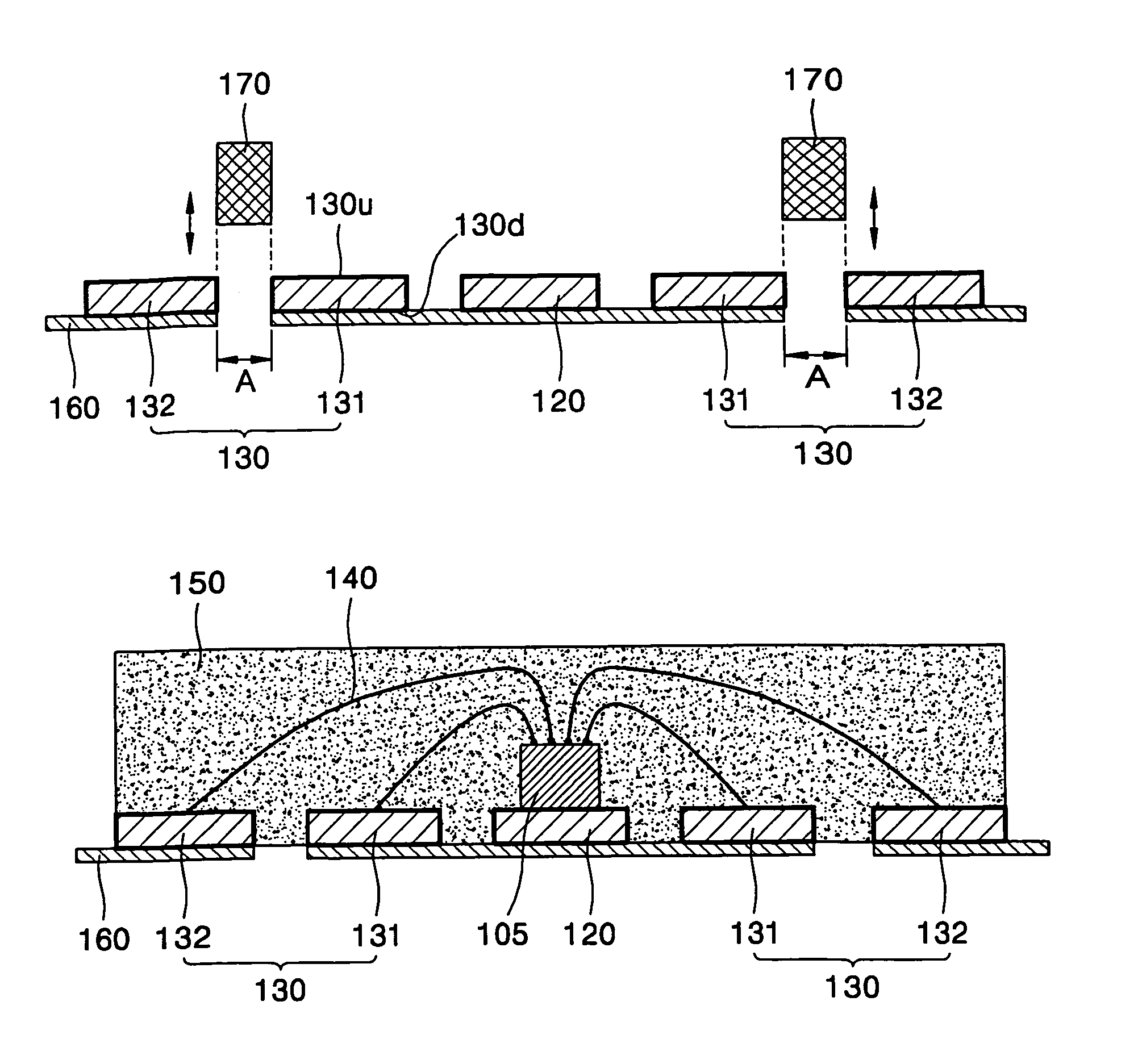
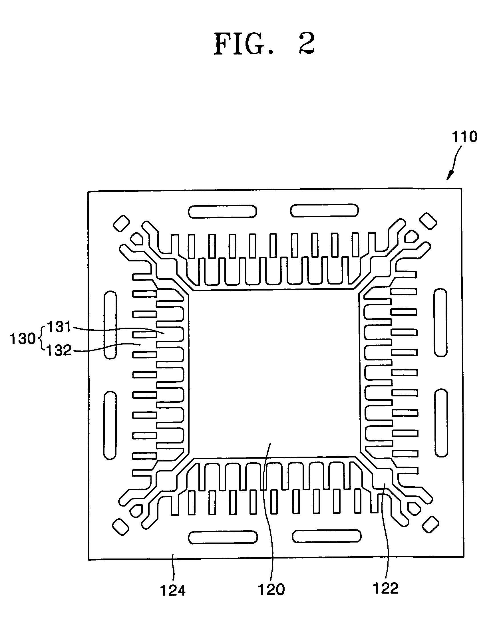
[0026]FIG. 2 shows an example of a lead frame for a semiconductor package, which includes two rows of leads. The lead frame includes a die pad 120 configured to mount a semiconductor chip thereon, and two rows of leads 130 arranged about the die pad 120. The die pad 120 is connected to an outer flame 124 by a pad supporter (a so-called tie bar) 122 and supports the semiconductor chip thereon.

[0027]The leads 130 include first rows of leads 131 and second rows of leads 132, each of the leads adapted to electrically connect the semiconductor chip to an external substrate (e.g., a PCB) as an input / output terminal. When an assembly process of the semiconductor package is completed, the outer frame 124 is to be removed.

[0028]FIG. 3 is a flowchart illustrating a method of manufacturing a semiconductor package having mul...


PUM


Abstract

Provided is a method of producing a semiconductor package including at least two rows of leads in which the leads of each row separately connecting a semiconductor chip to an external substrate. The method includes: forming a lead frame, the lead frame including a die pad and a plurality of leads arranged about the die pad; attaching an adhesive tape to a surface of the lead frame covering at least substantially the die pad and the plurality of leads; removing portions of the leads and the adhesive tape disposed in a dividing region and thereby separating at least some of the plurality of leads to form multiple rows of leads; and mounting a semiconductor chip on the die pad, electrically connecting the semiconductor chip with the lead frame, and molding the lead frame and the semiconductor chip to provide a semiconductor package. The adhesive tape attached at undesirable locations of the lead frame is preferably removed after provision of the semiconductor package.

Description

BACKGROUND OF THE INVENTION[0001]This application claims priority of Korean Patent Application No. 10-2004-0026247, filed on Apr. 16, 2004, in the Korean Intellectual Property Office, the disclosure of which is incorporated herein in its entirety by reference.[0002]1. Field of the Invention[0003]The present invention relates to a method of manufacturing a semiconductor package having a lead frame with multiple rows of leads arranged about a semiconductor chip of the semiconductor package.[0004]2. Description of the Related Art[0005]As semiconductor chips become more highly integrated, the number of input / output terminals for electrically interconnecting a semiconductor chip to an external PCB needs to be greatly increased. Accordingly, continuing research efforts have been made to develop a semiconductor package having a great number of leads, for example, at least two rows of leads arranged around the semiconductor chip in which the leads of each row are separately connected to a s...

Claims


Application Information

Patent Timeline
Patent Type & Authority Patents(United States)
IPC IPC(8): H01L23/495H05K5/02H01L21/48H01L21/60H01L21/56H01L21/68H01L23/31
CPCH01L21/4842H01L21/568H01L23/3107H01L23/49541H01L24/48H01L2924/01079H01L2924/01078H01L2924/01046H01L2224/85001H01L2224/48465H01L2224/48247H01L2224/48091H01L2924/00014H01L2924/00H01L2924/181H01L2924/00012H01L2224/45099H01L2224/45015H01L2924/207H04B1/40
Inventor KIM, JUNG-IL
Owner HAESUNG CO LTD
Learn More