Display device

a display device and display screen technology, applied in the field of display devices, can solve the problems of significant electric power consumption, reduced “h” level, and considerable drawbacks

Active Publication Date: 2007-02-06
SANYO ELECTRIC CO LTD
View PDF20 Cites 22 Cited by
  • Summary
  • Abstract
  • Description
  • Claims
  • Application Information

AI Technical Summary

Benefits of technology

[0014]This invention is directed to the smooth writing of data into the retaining circuit which retains the image signal data.

Problems solved by technology

Accordingly, it is necessary to operate a driver circuit which generates a driver signal for the scanning signals and the image signals, and an external LSI which generates various signals for controlling the timing of the driver circuit, resulting in a significant electric power consumption.
This is a considerable drawback when such a configuration is used in a cellular phone device which has only a limited power source.
However, the aforementioned liquid crystal display device has the following problem.
Therefore, the “H” level competes against “L” level, resulting in a reduced “H” level, and possibly causing a false writing.
However, because of the presence of the electric passage described above, this condition may not be fulfilled due to the decrease in the voltage of the source 11s of the pixel element selection TFT 72.
However, because of the presence of the electric passage described above, the condition mentioned above may not be fulfilled due to the increase of the voltage of the source 11s of the pixel element selection TFT 72.
Accordingly, a conventional device such as shown in FIG. 8 may not properly change the status of the retaining circuit, or may take a long time to change the status.

Method used


Image

  • Display device
  • Display device
  • Display device

Examples


first embodiment

[0035]The display device of this invention will be explained by referring to the circuit diagram shown in FIG. 1. This embodiment describes a case where this invention is applied to the liquid crystal display device.

[0036]On an insulating substrate (not shown in the figure), a gate signal line 51 and a drain signal line 61 are formed perpendicular to each other. Near the crossing of the signal lines, a pixel element selection TFT 72, connected to the both of the signal lines 51, 61, is also formed.

[0037]A retaining circuit 110 comprises first and second inverter circuits that form a positive feed back loop. A source 11s of the pixel element selection TFT 72 is connected to the input terminal of the first inverter circuit INV1 and its output is fed to the second inverter circuit INV2. The output of the second inverter circuit INV2 is connected to the input terminal of the first inverter circuit INV1.

[0038]The first inverter circuit INV1 is a CMOS type inverter circuit and comprises a...

second embodiment

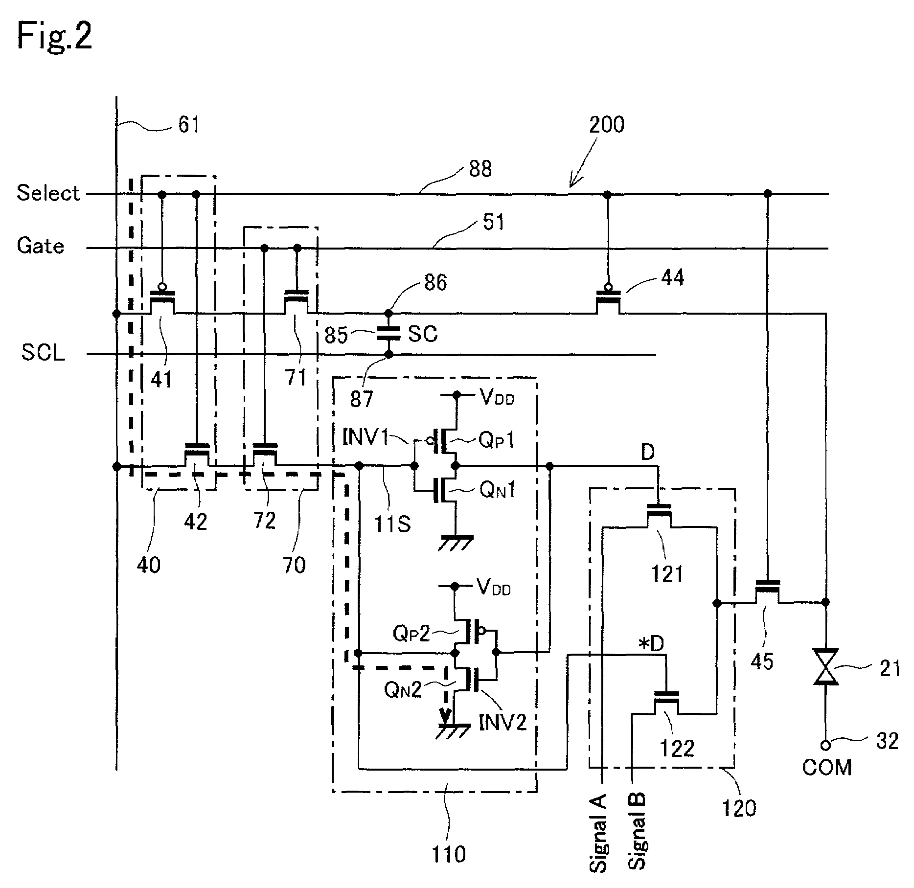
[0051]Next, this invention will be explained by referring to FIGS. 2 and 3. This embodiment also describes a case where this invention is applied to a liquid crystal display device. FIG. 2 is a circuit diagram showing the configuration of one pixel element 200. FIG. 3 is a circuit diagram of the whole display device including the pixel element 200. This display device is a liquid crystal display device capable of selecting between an analog display mode based on the analog image signal (full color moving picture) and a digital display mode based on the digital image signal retained in the retaining circuit 110 (still image).

[0052]On the insulating substrate 10 (not shown in the figure), a plurality of gate signal lines 51 connected to the gate driver 50, which supplies the scanning signal, are disposed in one direction. A plurality of drain signal lines 61 are also disposed in a direction perpendicular to the gate signal line 51.

[0053]Sampling transistors SP1, SP2, . . . , SPn turn ...


PUM

PropertyMeasurementUnit
voltageaaaaaaaaaa
voltagesaaaaaaaaaa
threshold voltageaaaaaaaaaa

Abstract

A digital image signal fed from the drain signal line is written into a retaining circuit through a pixel element selection TFT and a liquid crystal displays an image based on the digital image signal. In the retaining circuit, a threshold voltage of the first inverter circuit is set smaller than a threshold voltage of the second inverter circuit. Therefore, false writing of the image signal data into the retaining circuit can be prevented, leading to an accurate display the image signal retained in the retaining circuit.

Description

BACKGROUND OF THE INVENTION[0001]1. Technical Field of the Invention[0002]This invention relates to a display device, specifically to a display device which is incorporated into a portable communication and computing device.[0003]2. Background of the Invention[0004]There has been a great demand in the market for portable communication and computing devices such as a portable TV and a cellular phone. All these devices need a small, light-weight and low-power consumption display device, and efforts have been made accordingly.[0005]FIG. 6 shows a circuit diagram corresponding to a single pixel element of a conventional liquid crystal display device. A gate signal line 51 and a drain signal line 61 are placed on an insulating substrate (not shown) perpendicular to each other. A thin-film transistor (TFT) 65 connected to two signal lines 51, 61, is formed near the intersection of the two signal lines 51, 61. A source 11s of the TFT 65 is connected to a display electrode 80 of a liquid cr...

Claims


Application Information

Patent Timeline
Patent Type & Authority Patents(United States)
IPC IPC(8): G09G3/36G02F1/133
CPCG09G3/3648G09G3/3659G09G2300/0857G09G2300/0842G02F1/133
Inventor SENDA, MICHIRUYOKOYAMA, RYOICHI
Owner SANYO ELECTRIC CO LTD
Why Eureka
Try Eureka