EL display device providing means for delivery of blanking signals to pixel elements

a display device and blanking signal technology, applied in the field of electroluminescent display devices, can solve the problems of reducing the aperture ratio of pixels and the increase of dedicated transistors, and achieve the effect of excellent gray-scale performance and uniform display

Inactive Publication Date: 2007-02-06
JOLED INC
View PDF26 Cites 34 Cited by
  • Summary
  • Abstract
  • Description
  • Claims
  • Application Information

AI Technical Summary

Benefits of technology

[0026]With this configuration, an EL display device with excellent gray-scale performance can be configured.
[0037]According to a fifteenth aspect of the present invention, the EL display device of the thirteenth aspect may be such that the designated gate line is an antecedent gate line.
[0038]As with the effects of the fourth aspect of the present invention, a change in the potential of the pixel electrodes, resulting from the parasitic capacitors of the transistors, can be suppressed without the need to add a large storage capacitor.
[0039]According to a sixteenth aspect of the present invention, the EL display device of the thirteenth aspect may be such that the sum of impedance of the designated gate line and output impedance of a buffer in last stage in the gate line driver circuit connected to the designated gate line is 20% or less of impedance of the EL elements connected to the designated gate line.
[0040]The reason for controlling the impedance is that when the impedance exceeds 20%, the potential of the ends of the gate lines decreases and a sufficient voltage cannot be applied to the EL elements, and accordingly a uniform display cannot be obtained.
[0041]According to a seventeenth aspect of the present invention, the EL display device of the thirteenth aspect may be such that: each of the unit pixels is split into a plurality of sub-pixels; the sub-pixels each individually have a sub-pixel electrode, a switching transistor, a controlling transistor, an auxiliary capacitor, and a gate line; and gray-scale display is provided by combination of ON / OFF states of each of the sub-pixels, and a blanking signal is provided to each of the sub-pixels via the gate line.

Problems solved by technology

Thus, an increase in the area occupied by the dedicated transistors and controlling lines reduces the aperture ratio of the pixels.

Method used


Image

  • EL display device providing means for delivery of blanking signals to pixel elements
  • EL display device providing means for delivery of blanking signals to pixel elements
  • EL display device providing means for delivery of blanking signals to pixel elements

Examples


embodiment 1

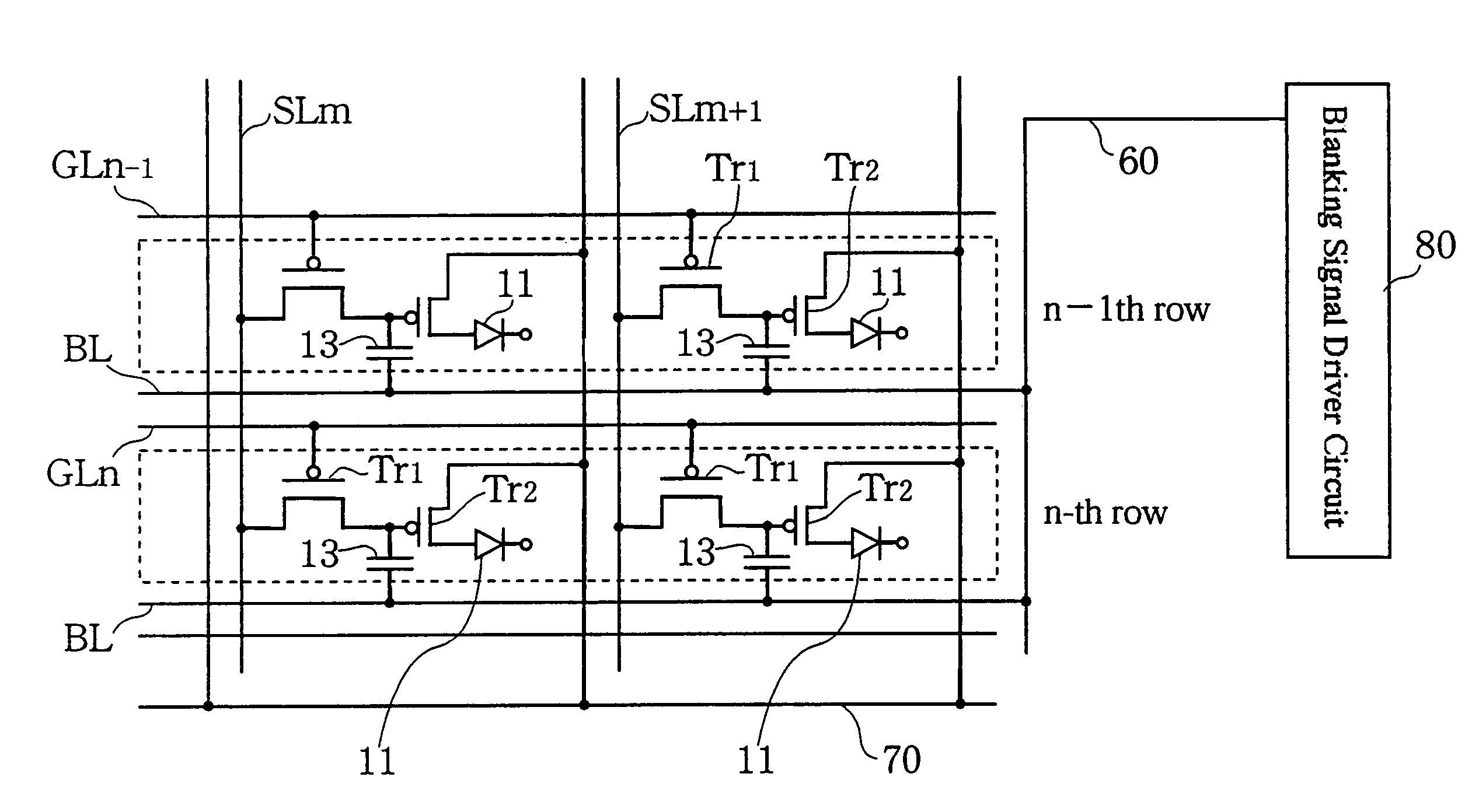
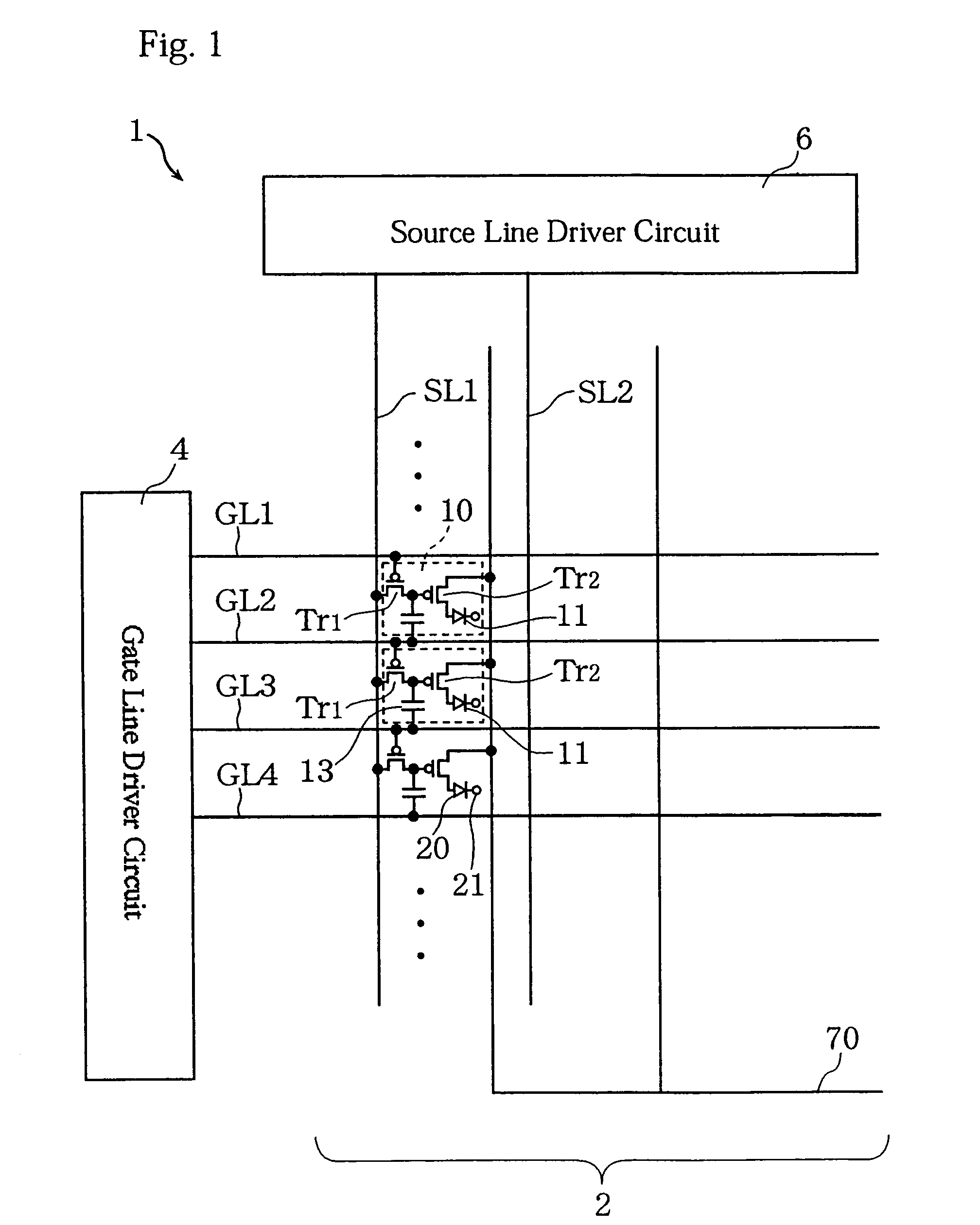
[0084]FIG. 1 is a circuit diagram showing the configuration of an active matrix type EL display device according to Embodiment 1. An active matrix type EL display device 1 includes a display portion 2 having unit pixels 10 arranged in a matrix, a gate line driver circuit 4 for outputting scan signals to each of the unit pixels 10 via gate lines GL1, GL2, . . . (reference symbol GL will be used when collectively referring to the gate lines), a source line driver circuit 6 for outputting image signals to each of the unit pixels 10 via source lines SL1, SL2, . . . (reference symbol SL will be used when collectively referring to the source lines), and a current-supplying line 70 for supplying a current to each EL element 11.

[0085]The unit pixels 10 each includes the EL element 11, serving as an emitter of the unit pixel, a switching transistor Tr1, a driver transistor Tr2 for controlling the amount of driving current provided to the EL element 11, and an auxiliary capacitor 13. The auxi...

embodiment 2

[0105]FIG. 8 is a cross-sectional view showing the configuration of a pixel of an active matrix type EL display device according to Embodiment 2. Embodiment 2 is characterized in that transistors Tr1 and Tr2 are both N-channel transistors and that a cathode electrode of an EL element serves as a pixel electrode and an anode electrode serves as a counter electrode, except for which the configuration is the same as that of the foregoing Embodiment 1. In Embodiment 2, the cathode electrode is an opaque electrode and the anode electrode is an ITO electrode. With such a configuration, light from a light-emitting layer is irradiated from the other side from a substrate 35. Thus, in Embodiment 2, the substrate 35 does not necessarily need to be a transparent substrate, as in Embodiment 1, and it is possible to use an opaque substrate such as silicon.

[0106]In the case where the cathode electrode of the EL element serves as a pixel electrode and the anode electrode serves as a counter electr...

embodiment 3

[0112]FIG. 11 is a plane view of a display portion of a display device according to Embodiment 3, and FIG. 12 is a circuit diagram of the display portion. FIGS. 11 and 12 show only the configuration of a pixel. Embodiment 3 is characterized in that one unit pixel is split into a plurality of regions and that gray-scale display is provided by a spatial dithering method. The specific configuration is described below with reference to FIGS. 11 and 12.

[0113]A unit pixel 10 is structured such that it is split into a plurality of regions (four-regions in Embodiment 3). The configuration of sub-pixels 50, split regions, is the same as that of the unit pixel 10 in the foregoing Embodiment 1. Specifically, each of the sub-pixels 50 has a gate line GL, a switching transistor Tr1, a driver transistor Tr2, and an auxiliary capacitor 13.

[0114]Gray-scale display can be realized by the combination of light-emission and non-light-emission of the split sub-pixel regions. To the source line SL, a dig...


PUM


Abstract

An EL display device 1 includes a display portion 2 having unit pixels 10 arranged in a matrix, a source line driver circuit 6, and a gate line driver circuit 4. Each of the unit pixels 10 has an EL element 11, a switching transistor Tr1, a driver transistor Tr2, and an auxiliary capacitor 13. The auxiliary capacitor 13 has electrodes, one connected to a gate electrode of the transistor Tr2 and the other to a next gate line GL. The gate line driver circuit 4 outputs, via the next gate line GL, blanking signals for forcibly stopping a light-emitting state of the EL elements 11, within hold times in which the voltages written to the gate electrodes of the transistors Tr2 are held. With such a configuration, a blanking period where the EL elements do not emit light, is inserted in one frame.

Description

TECHNICAL FIELD[0001]The present invention relates to an EL (electroluminescent) display device.BACKGROUND ART[0002]The configuration of a unit pixel of a prior-art EL display device is shown in FIGS. 32 and 33. In FIGS. 32 and 33, reference symbol GL indicates a gate line, reference numeral 13 indicates an auxiliary capacitor, reference symbol SL indicates a source line, reference numeral 11 indicates an EL element, reference symbol Tr1 indicates a switching transistor, reference symbol Tr2 indicates a driver transistor, and reference numeral 70 indicates a current-supplying line for supplying a current to the EL element 11. The EL element 11 emits light as follows. First, when the gate line GL and the source line SL are both turned on, an electric charge is stored in the auxiliary capacitor 13 via the switching transistor Tr1. Since the auxiliary capacitor 13 continues to apply a voltage to a gate of the driver transistor Tr2, even when the switching transistor Tr1 is turned off, ...

Claims


Application Information

Patent Timeline
Patent Type & Authority Patents(United States)
IPC IPC(8): G09G5/00G09G3/20G09G3/30G09G3/32
CPCG09G3/3258G09G3/3266G09G3/2011G09G2320/0261G09G2300/0443G09G2300/0465G09G2300/0804G09G2300/0814G09G2300/0828G09G2300/0842G09G2300/0866G09G2300/0876G09G2310/0254G09G2310/061G09G2320/0257G09G3/2074
Inventor NANNO, YUTAKASENDA, KOUJI
Owner JOLED INC
Why Eureka
Try Eureka