

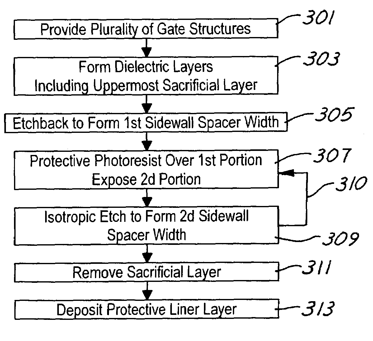
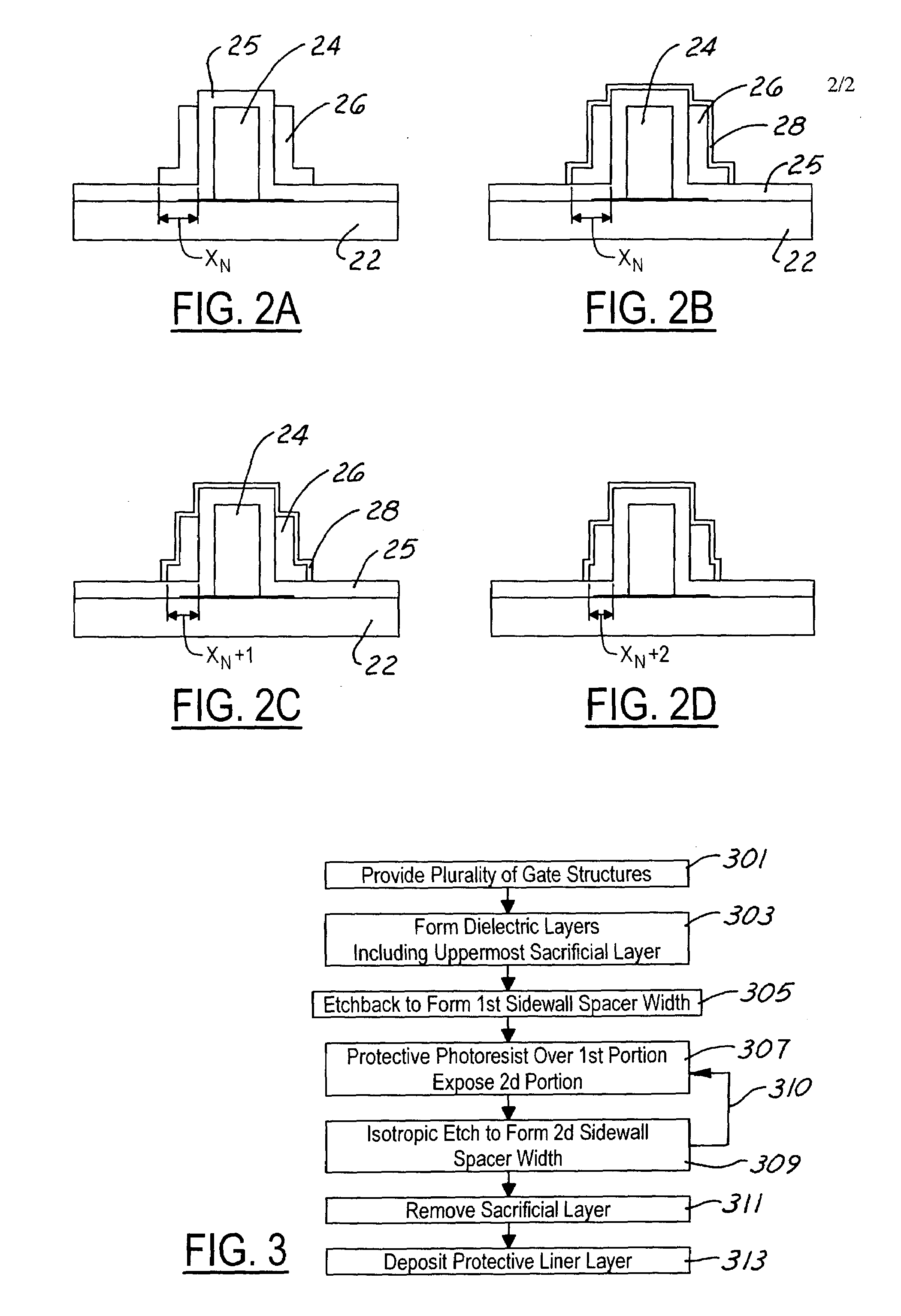
Method for multiple spacer width control
a technology of spacer width and control method, which is applied in the direction of cable/conductor manufacturing, semiconductor device fabrication, electrical apparatus, etc., can solve the problem of excessive number of photoresist patterning processes
- Summary
- Abstract
- Description
- Claims
- Application Information
AI Technical Summary
Problems solved by technology
Method used
Image

Examples
Embodiment Construction
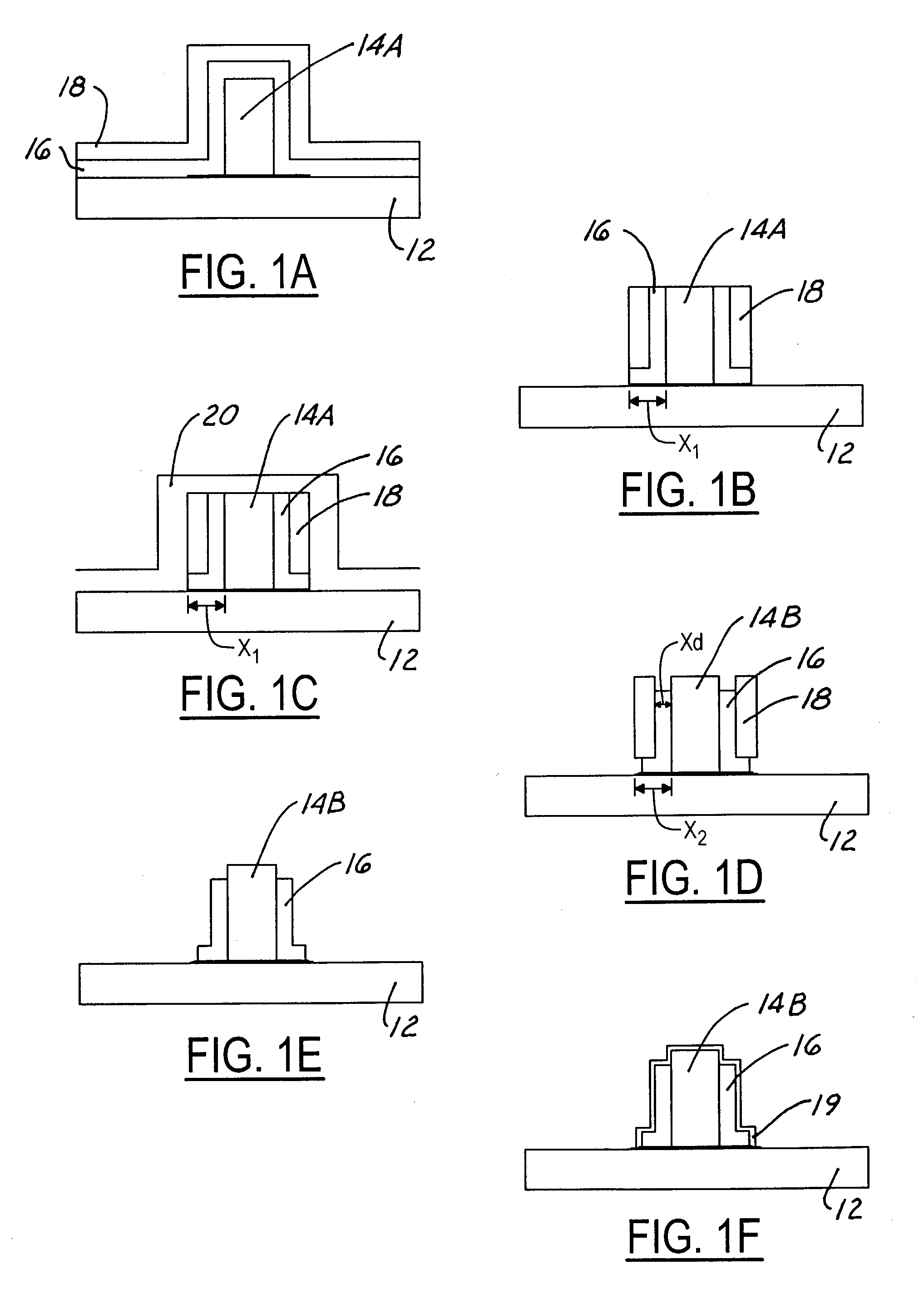
[0012]While the method of the present invention is explained with reference to formation of gate sidewall spacers it will be understood that the method of the present invention may be adapted for the formation of spacers in the formation of any semiconductor structure.
[0013]Referring to FIG. 1A is shown a substrate 12, for example silicon, silicon on insulator (SOI), silicon oxide (e.g., SiO2), silicon nitride (e.g., SiN), or silicon oxynitride (e.g., SiON). Overlying the substrate 12 is shown gate structure 14A. Although the details of the gate structure are not shown, the gate structure typically includes one or more gate dielectric layers formed over the substrate. A conductive gate material such as polysilicon, metal or SiGe is then deposited followed by a photolithographic patterning process to define the gate structure, and a plasma etching process, for example a polysilicon dry etching process, to form the gate 14A. It will be appreciated that the gate structure may include s...
PUM
 Abstract
Description
Claims
Application Information