Optical element, thin film structure, optical switch, and method of manufacturing optical element
- Summary
- Abstract
- Description
- Claims
- Application Information
AI Technical Summary
Benefits of technology
Problems solved by technology
Method used
Image

Examples
first embodiment
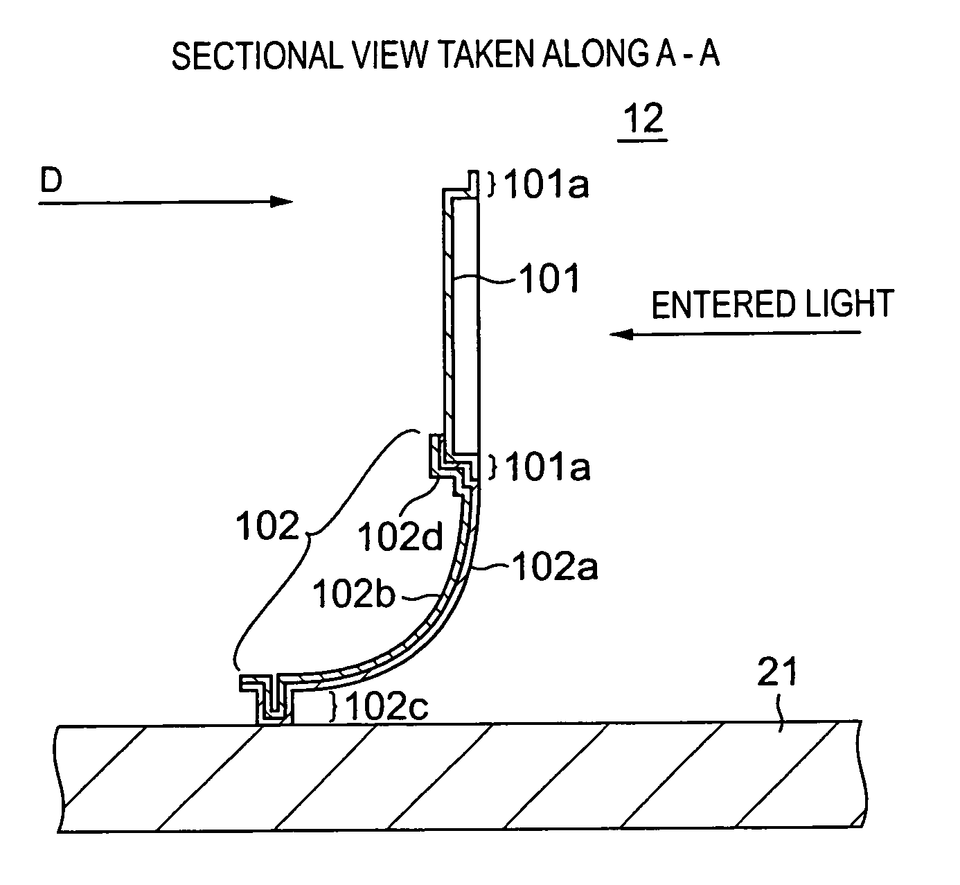
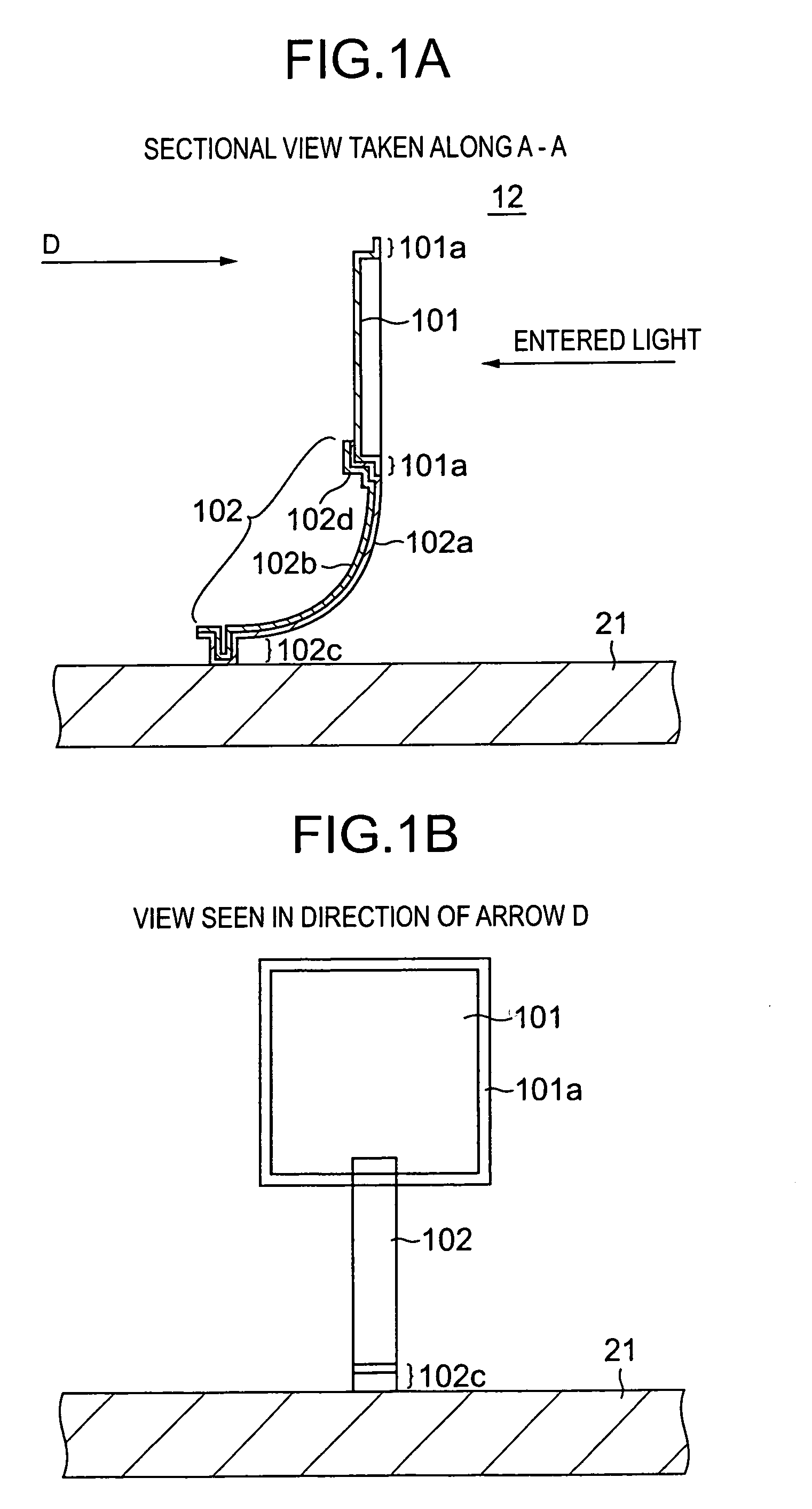
[0186]An optical switch in the first embodiment will be described with reference to FIGS. 1A and 1B, FIG. 2, FIG. 3 and FIG. 4.
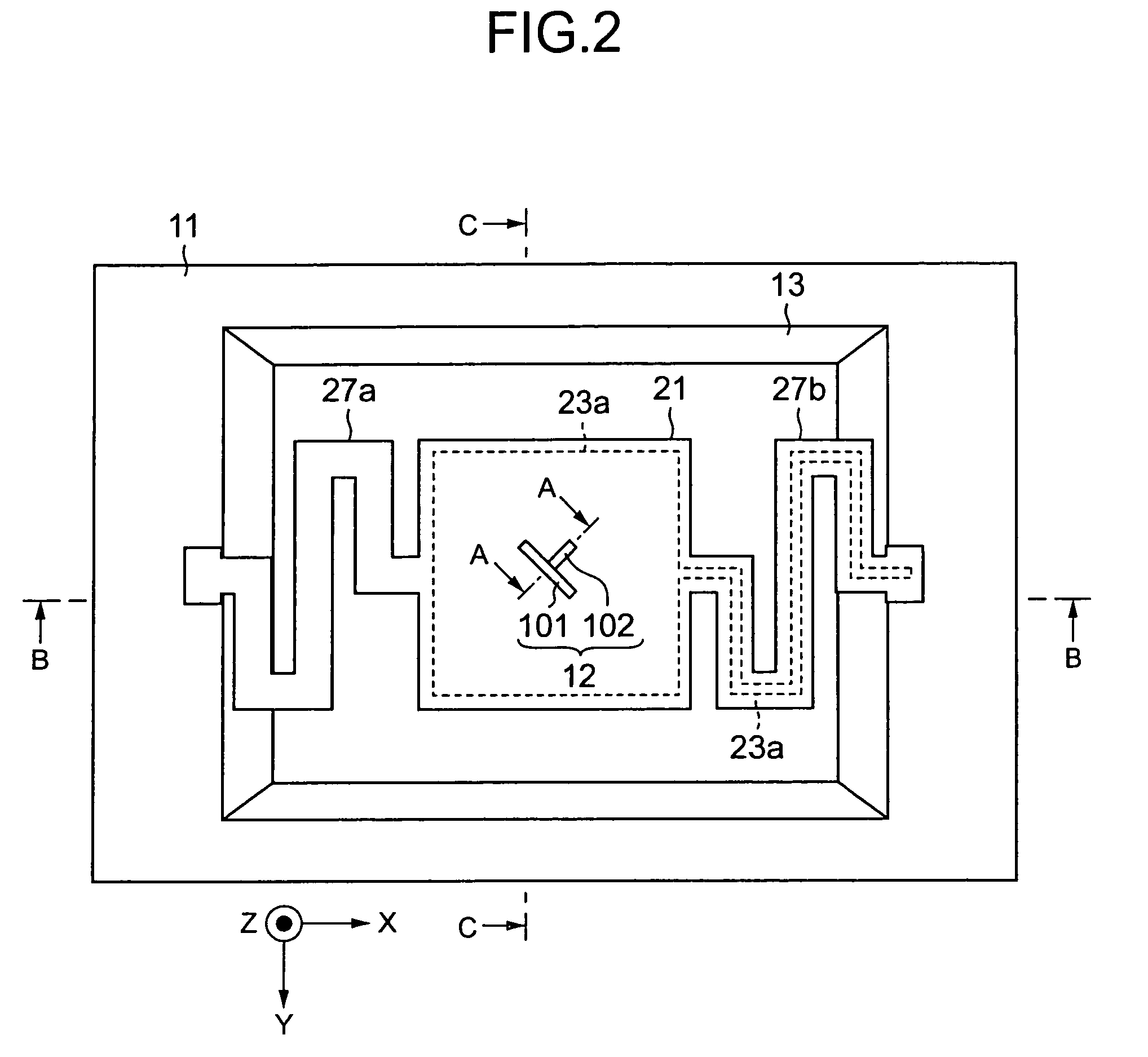
[0187]As shown in FIG. 2, FIG. 3 and FIG. 4, the optical switch includes a semiconductor substrate 11 which is formed with a recess 13, a movable plate 21, and two spring portions 27a, 27b which support the movable plate 21 over the substrate 11. A mirror 12 is mounted on the movable plate 21. A temperature regulation element (not shown), for example, Peltier element is arranged under the substrate 11 in order to keep the temperature of the mirror 12 at a preset temperature.
[0188]As shown in FIGS. 1A and 1B, the mirror 12 is constructed of a reflection portion 101, and a support portion 102 which supports the reflection portion 101 over the movable plate 21. The reflection portion 101 is made of an Al (aluminum) film. The outer edge part of the Al film of the reflection portion 101 is formed with a stepped structure in order to afford rigidity, thereby to fo...
second embodiment
[0203]Next, an optical switch in the second embodiment will be described with reference to FIGS. 10A and 10B.
[0204]The optical switch in the second embodiment is such that a mirror 112 in FIGS. 10A and 10B is mounted on a movable plate 21 instead of the mirror 12 of the optical switch in the first embodiment. Since the construction of the optical switch except the mirror 112 is the same as in the first embodiment, it shall be omitted from description.
[0205]Likewise to the mirror 12 in the first embodiment, the mirror 112 in the second embodiment is so constructed that a reflection portion 101 is supported by bent support portion 102. As shown in FIG. 10B, however, the reflection portion 101 is shaped so as to be bilaterally stretched out in the direction of its principal plane, and it is supported by three support portions 102. The film structure of the reflection portion 101, and that of each support portion 102 are the same as in the first embodiment.
[0206]Besides, two stop portio...
third embodiment
[0213]Next, an optical switch in the third embodiment will be described with reference to FIG. 12.
[0214]The optical switch in the third embodiment is such that a mirror 113 in FIG. 12 is mounted on a movable plate 21 instead of the mirror 12 of the optical switch in the first embodiment. Since the construction of the optical switch except the mirror 113 is the same as in the first embodiment, it shall be omitted from description.
[0215]Although the mirror 113 in the third embodiment is structurally similar to the mirror 112 in the second embodiment, it differs from the mirror 112 in the point that stop portions 93, 94 are further arranged at positions at which they confront respective stop portions 91, 92 with a reflection portion 101 held therebetween (the stop portion 94 is not shown in FIG. 12). The shapes of the reflection portion 101 and the stop portions 91, 92, 93, 94 before the removal of resist layers 81, 82 being sacrificial layers are shown in FIG. 13. Likewise to the stop...
PUM
 Abstract
Description
Claims
Application Information
 - R&D Engineer
- R&D Manager
- IP Professional
- Industry Leading Data Capabilities
- Powerful AI technology
- Patent DNA Extraction
Browse by: Latest US Patents, China's latest patents, Technical Efficacy Thesaurus, Application Domain, Technology Topic.
© 2024 PatSnap. All rights reserved.Legal|Privacy policy|Modern Slavery Act Transparency Statement|Sitemap