
Array substrate having color filter on thin film transistor structure for LCD device and method of fabricating the same

a thin film transistor and color filter technology, applied in the direction of static indicating devices, identification means, instruments, etc., can solve the problems of deteriorating the image quality of the lcd device, achieve simplified and stabilized fabricating processes, increase manufacturing yield, and high aperture ratio

Inactive Publication Date: 2007-02-20
LG DISPLAY CO LTD
View PDF7 Cites 32 Cited by
  • Summary
  • Abstract
  • Description
  • Claims
  • Application Information

AI Technical Summary

Benefits of technology

[0019]An object of the present invention is to provide an array substrate for a liquid crystal display device that provides a high aperture ratio.
[0020]Another object of the present invention is to provide a method of fabricating an array substrate for a liquid crystal display device having simplified and stabilized fabricating processes and to increase manufacturing yield.

Problems solved by technology

Moreover, if there are errors in the aligning margin of the black matrix 6, the light leakage still occurs within the open spaces A and B, and deteriorates the image quality of the LCD device.

Method used


Image

  • Array substrate having color filter on thin film transistor structure for LCD device and method of fabricating the same
  • Array substrate having color filter on thin film transistor structure for LCD device and method of fabricating the same
  • Array substrate having color filter on thin film transistor structure for LCD device and method of fabricating the same

Examples


Embodiment Construction

[0047]Reference will now be made in detail to the preferred embodiments of the present invention, examples of which are illustrated in the accompanying drawings.

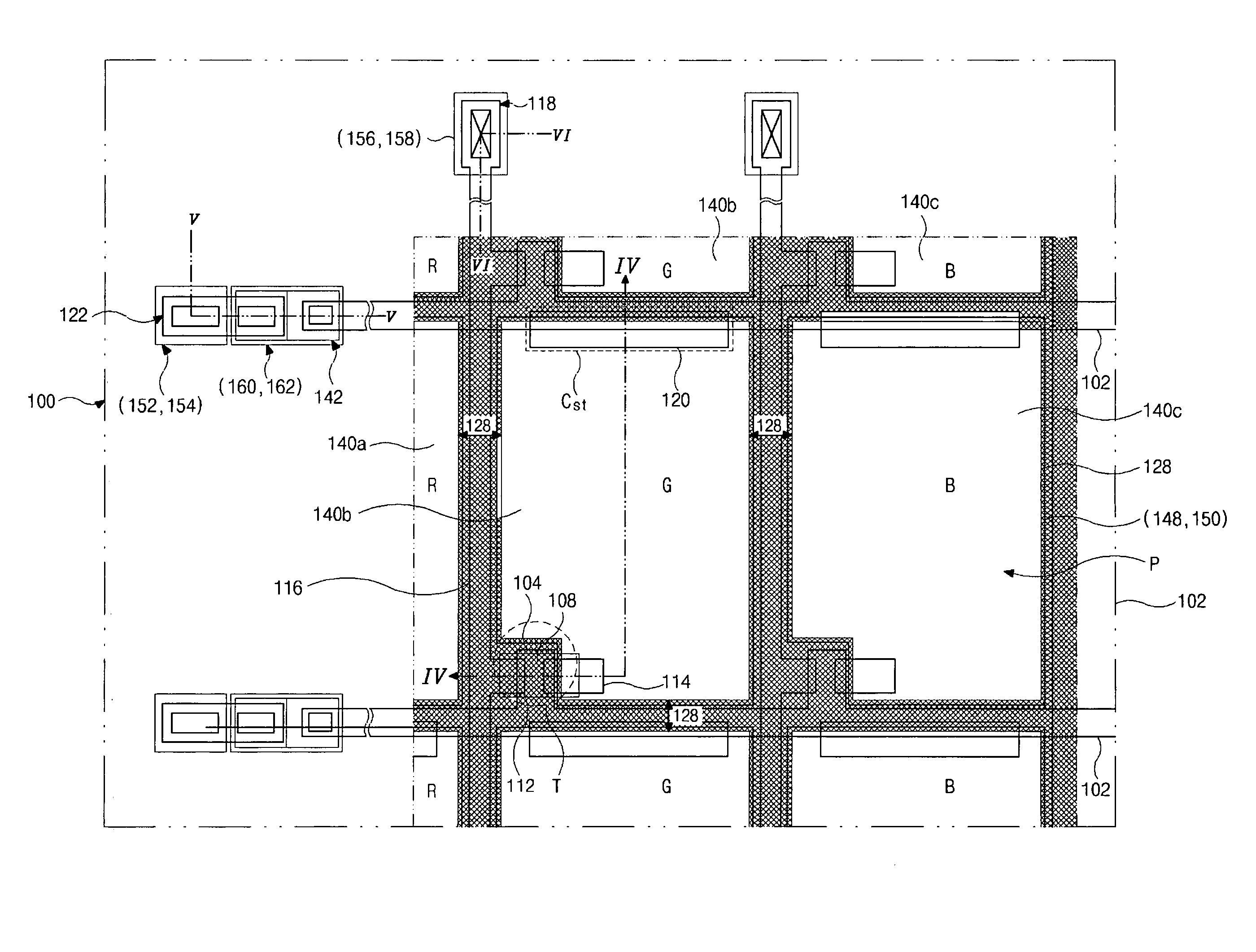
[0048]FIG. 3 is a plan view of an exemplary array substrate having a color filter on thin film transistor structure according to the present invention. In FIG. 3, an array substrate 100 may include a plurality of gate lines 102 disposed along a first direction and a plurality of data lines 116 disposed along a second direction perpendicular to the first direction. Accordingly, the plurality of gate lines 102 and the plurality of data lines 116 cross one another to define a plurality of pixel regions P. Each of the data lines 116 may include a data pad 118 disposed at least at one end of the data lines 116, and each of the gate lines 102 may include a gate pad 122 disposed at least at one end of the gate lines 102. Alternatively, multiple data and gate pads 118 and 122 may be disposed at opposing ends of the data and gate lin...


PUM

PropertyMeasurementUnit
transparentaaaaaaaaaa
transparent conductiveaaaaaaaaaa
colorsaaaaaaaaaa

Abstract

An array substrate device includes a gate line formed on a substrate extending along a first direction having a gate electrode, a data line formed on the substrate extending along a second direction having a data pad disposed apart from a first end of the data line, the data and gate lines defining a pixel region, a gate pad formed on the substrate disposed apart from a first end of the gate line, a thin film transistor formed at a crossing region of the gate and data lines and including the gate electrode, a semiconductor layer, a source electrode, and a drain electrode, a black matrix overlapping the thin film transistor, the gate line, and the data line except for a first portion of the drain electrode, a first pixel electrode at the pixel region contacting the first portion of the drain electrode and the substrate, a color filter on the first pixel electrode at the pixel region, and a second pixel electrode on the color filter contacting the first pixel electrode.

Description

[0001]The present invention claims the benefit of Korean Patent Application Nos. P2002-0078007 and P2002-0078910 filed in Korea on Dec. 9, 2002 and Dec. 11, 2002, respectively, which are hereby incorporated by reference.BACKGROUND OF THE INVENTION[0002]1. Field of the Invention[0003]The present invention relates to a liquid crystal display device and a method of fabricating a liquid crystal display device, and more particularly, to an array substrate having a color filter on thin film transistor structure and a method of fabricating an array substrate having a color filter on thin film transistor structure.[0004]2. Discussion of the Related Art[0005]In general, since flat panel display devices are thin, light weight, and have low power consumption, they are commonly used in portable devices. Among the various types of flat panel display devices, liquid crystal display (LCD) devices are commonly used in laptop and desktop computer monitors because of their superior resolution, color ...

Claims


Application Information

Patent Timeline
Patent Type & Authority Patents(United States)
IPC IPC(8): G02F1/1335G02B5/20G02F1/133G02F1/1343G02F1/1362G02F1/1368G09F9/30H01L21/336H01L29/786
CPCG02F1/134336G02F1/13458G02F1/136209H01L27/1288H01L27/1214H01L29/78633G02F2001/136222G02F1/136222G02F1/1335G02F1/1362
Inventor CHANG, YOUN-GYOUNGPARK, SEUNG-RYULLKIM, WOONG-KWONLEE, JONG-HWAE
Owner LG DISPLAY CO LTD
Features
  • Generate Ideas
  • Intellectual Property
  • Life Sciences
  • Materials
  • Tech Scout
  • Unparalleled Data Quality
  • Higher Quality Content
  • 60% Fewer Hallucinations
Learn More