

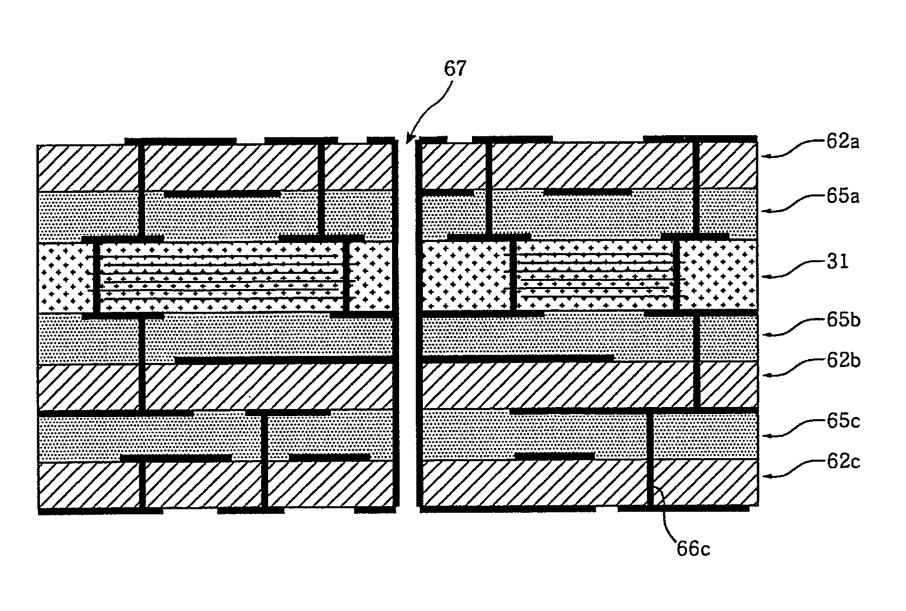
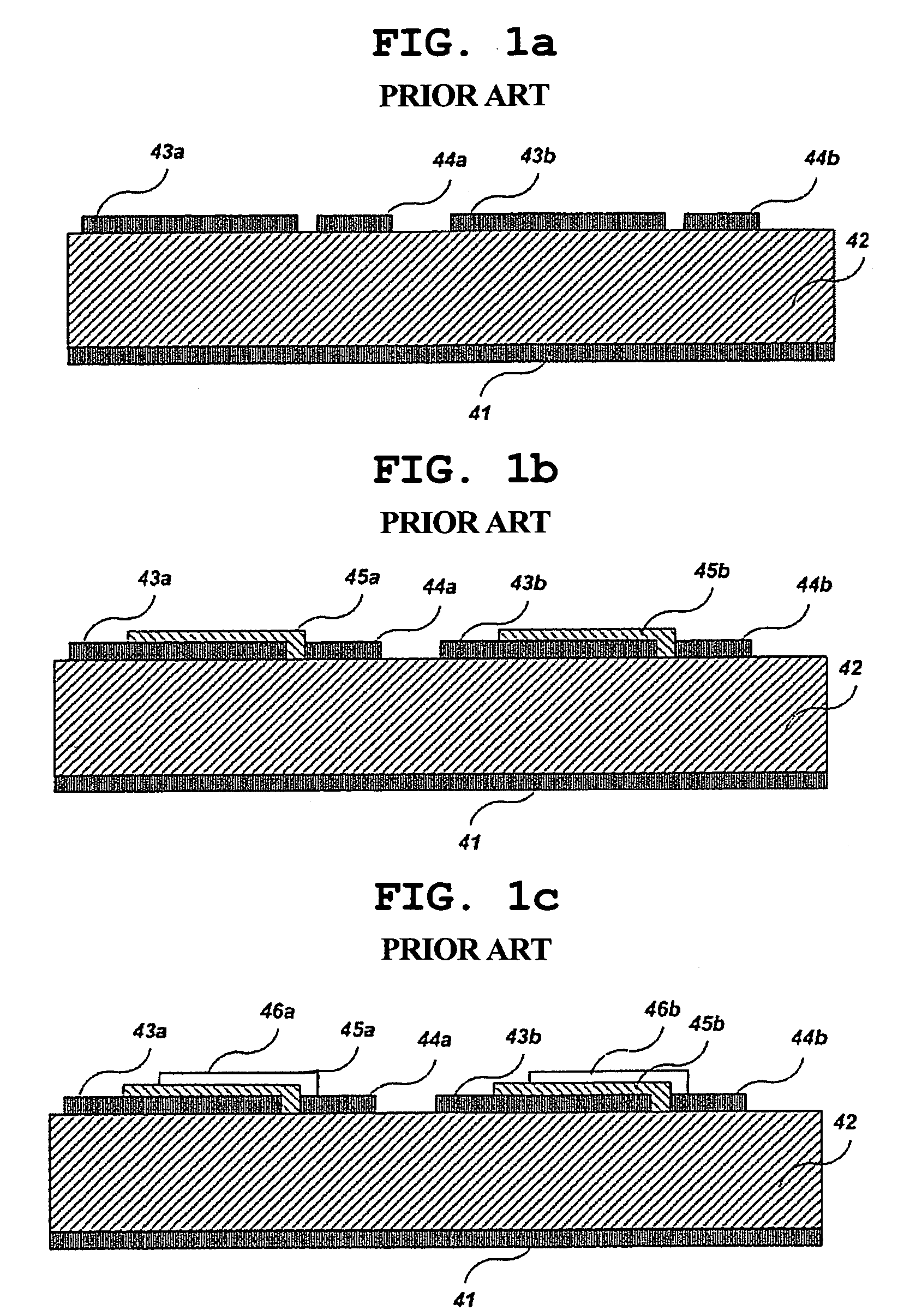
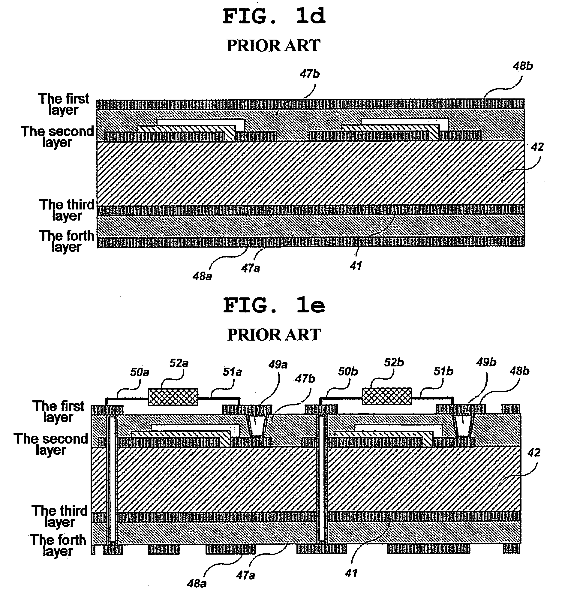
Printed circuit board including embedded capacitors and method of manufacturing the same
a technology of embedded capacitors and printed circuit boards, which is applied in the direction of printed capacitor incorporation, printed circuit non-printed electric components association, printed capacitor incorporation, etc., can solve the problems of reducing the mounting area of passive components on the pcb, insufficient value to completely embed capacitors in the pcb, and limitations on reducing the mounting area of passive components, so as to achieve the effect of drastically reducing the area for mounting passive components
- Summary
- Abstract
- Description
- Claims
- Application Information
AI Technical Summary
Benefits of technology
Problems solved by technology
Method used
Image

Examples
Embodiment Construction
[0038]Hereinafter, a detailed description will be given of the present invention, with reference to the appended drawings.
[0039]FIGS. 2, 3a, 3b, 4, and 5a to 5d show a process of manufacturing a PCB including embedded capacitors, according to an embodiment of the present invention.
[0040]As shown in FIG. 2, a conductor 23, such as aluminum or copper, is patterned into a predetermined pattern on a wide flat polymer sheet 22 having a high dielectric constant, to form a polymer condenser layer 21.
[0041]The patterning method of the conductor 23 includes, for example, a dry process such as sputtering, and a wet process such as screen printing.
[0042]In FIG. 3a, a first polymer condenser layer 21a having a first conductor pattern 23a and a second polymer condenser layer 21b having a second conductor pattern 23b are aligned and then laminated together. As is apparent from FIG. 3a, the first and second conductor patterns 23a and 23b of the first and second condenser layers 21a and 21b, respec...
PUM
| Property | Measurement | Unit |
|---|---|---|
| dielectric constant | aaaaa | aaaaa |
| dielectric constant | aaaaa | aaaaa |
| dielectric constant | aaaaa | aaaaa |
Abstract
Description
Claims
Application Information