Semiconductor device for sensor system

Inactive Publication Date: 2007-03-06
HITACHI LTD
View PDF10 Cites 63 Cited by
  • Summary
  • Abstract
  • Description
  • Claims
  • Application Information

AI Technical Summary

Benefits of technology

[0019]Under such circumstances, it is an object of the present invention to provide a semiconductor device that is employable for compact and light-weight sensor systems, each of w

Problems solved by technology

The functions of these PVA instruments are similar to those of conventional expensive medical measuring instruments.
The instrument thus comes to become very heavy (up to a few hundreds of grams).
Because a plurality of semiconductor circuits and other circuits are assembled on a board, it is unavoidable that the instrument will increase in size to a certain extent (up to the card size).
Consequently, the burden on the user increases, particularly when the user uses the PVA instrument for a long time.
In addition, because the PVA instrument is powered by a battery, the user is required to periodically replace the battery.
And, while each sensor is connected to the main board wirelessly through a low power wireless interface, each sensor is also connected to the sensor board through an ordinary wire, so that the PVA instrument comes to face some minor difficult

Method used


Image

  • Semiconductor device for sensor system
  • Semiconductor device for sensor system
  • Semiconductor device for sensor system

Examples


first embodiment

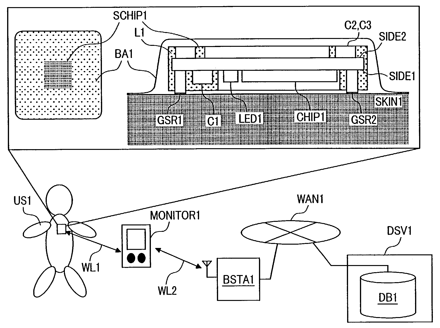
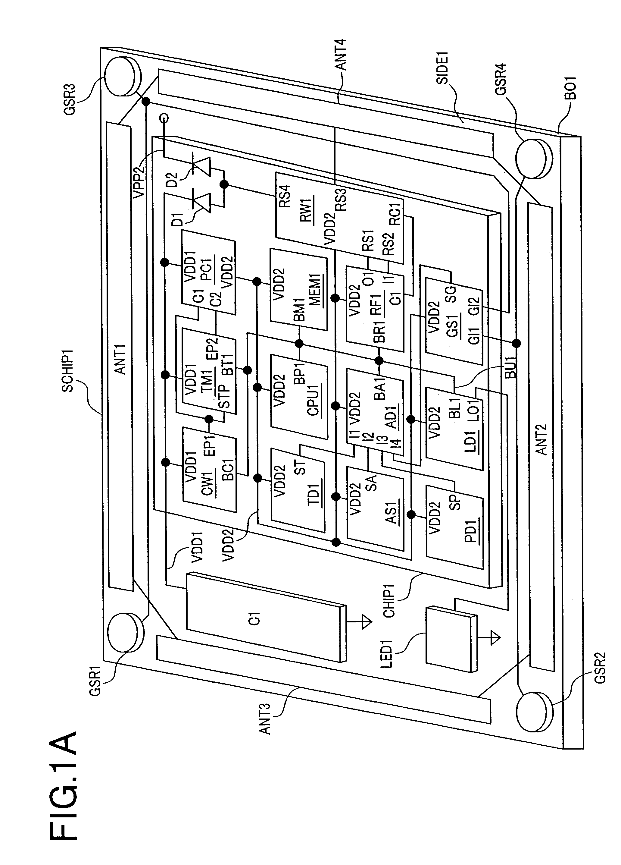
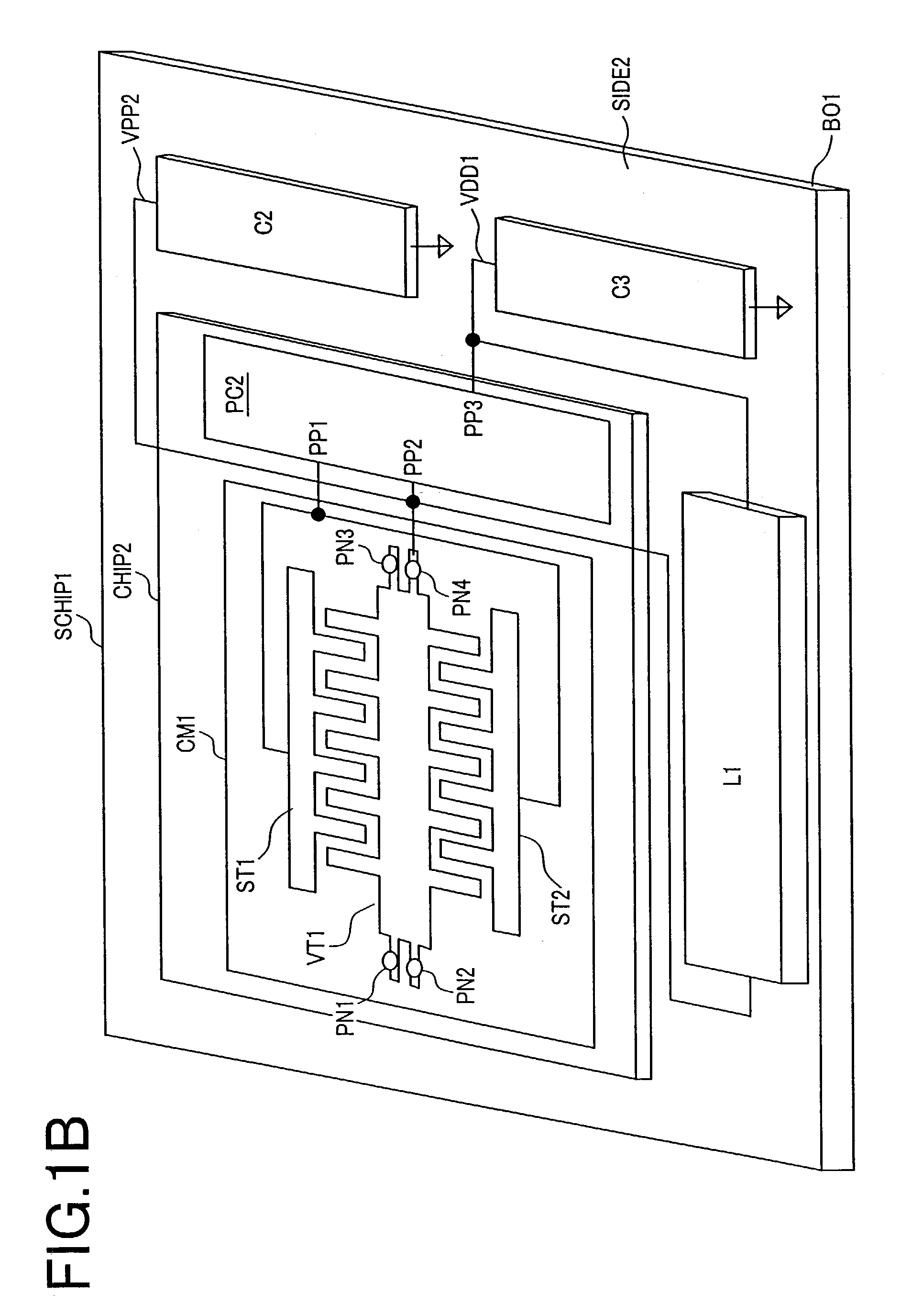
[0067]FIGS. 1A and 1B are block diagrams of a semiconductor device for a sensor system, that is, a sensor chip. FIG. 1A shows one main side (SIDE1) of the sensor chip, while FIG. 1B shows the other main side (SIDE2), that is the back side thereof. The sensor chip (SCHIP1) comprises a first semiconductor integrated circuit (CHIP1), a second semiconductor integrated circuit (CHIP2), a light emission diode (LED) chip (LED1), capacitors (C1 to C3), an inductor (L1), and a substrate (BO1) for mounting those chips and parts. The substrate (BO1) has wiring patterns for the connection among those chips, antenna patterns (ANT1 to 4) for use by a high frequency transmission / reception circuit (to be described later), and electrode patterns (GSR1 to 4) for use by a sensor circuit (GS1) (to be described later). Those patterns are formed with such metal materials as copper, gold, or the like. The chips and patterns are similar to those used usually for MCP (Multi Chip Package) chips.

[0068]FIGS. 2...

second embodiment

[0120]In the first embodiment, the MCP configuration is employed for the sensor chip of the present invention. On the other hand, the MEMS process is compatible with the semiconductor process, so that the MEMS variable capacitor can be integrated with other circuits, such as the sensors, the microprocessor, etc. on one chip. FIG. 22 shows a sensor chip in which the MEMS variable capacitor is integrated together with such other circuits as sensors, a microprocessor, etc. The sensor chip can also be reduced in size even in such a configuration. However, the MEMS variable capacitor is required to have a comparatively large area. If the sensor chip has a configuration as shown in FIG. 22 and a large MEMS variable capacitor is used, therefore, it is difficult to reduce the sensor chip in size.

[0121]FIG. 23A through FIG. 23C show a favorable configuration of such a sensor chip to reduce its size. In FIGS. 23A through 23C, the configurations of the PC1, PC2, and CPU1 circuits are the same ...

third embodiment

[0124]In the first embodiment, the MCP configuration specific to the sensor chip of the present invention is employed to integrate a small power generator that uses a MEMS variable capacitor, sensors, a microprocessor, a memory, a high frequency circuit, a power supply control circuit, etc. in a sensor chip to realize a compact and light-weight health care instrument. On the other hand, there is also a power generator or battery that can supply an electric power of 0.1 mW or so in a size roughly equal to that described above.

[0125]For example, FIGS. 24A and 24B show an example of a sensor chip that uses a power generator that makes good use of electromagnetic induction. FIG. 24A shows a side cross-sectional view of the chip and FIG. 24B shows a planar cross-sectional view of the chip. This power generator has the same configuration as that disclosed in the above-referenced document 11. A cavity CA1 is formed on the SIDE2 of the substrate BO2. A permanent magnet MA1 and a supporting ...


PUM


Abstract

A semiconductor device is employable for a compact and light-weight sensor system that is free of the need for battery replacement. The semiconductor device has a sensor chip (SCHIP1) comprising sensors (TD1, AS1, PD1, GS1), an A/D conversion circuit (AD1), a microprocessor (CPU1), a memory (MEM1), a transmission circuit (RF1), and a power generation circuit (CM1). The sensors, the A/D conversion circuit, the microprocessor, the memory, and the transmission circuit are formed on one side (SIDE1) of a substrate, while the power generation unit is formed on the other side (SIDE2) of the substrate.

Description

BACKGROUND OF THE INVENTION[0001]The present invention relates to a semiconductor device for use in sensor systems. More particularly, the present invention relates to a semiconductor device to be employed for compact and light sensor systems that are free of the need for battery replacement.[0002]In recent years, people have come to be more mindful of requisites to good health; and, accordingly, they are seeing the need for various personal vital assistant instruments (hereinafter, to be described as “PVA” instruments) that facilitate the users in making it easier to perform health checks by themselves. The functions of these PVA instruments are similar to those of conventional expensive medical measuring instruments. However, unlike those expensive medical instruments, such PVA instruments need to be supplied at lower prices, so that the general public is able to purchase them. In addition, for patients of lifestyle-related illnesses, it is important for them to monitor their bodi...

Claims


Application Information

Patent Timeline
IPC IPC(8): A61B5/00G01P15/125A61B5/01A61B5/0205A61B5/024A61B5/0245A61B5/053A61B5/11A61B5/145A61B5/1455G01D9/00G01K7/01G01N33/483G01N33/50G08C15/00G08C17/00H01L23/34H01L35/32
CPCA61B5/0002G01D9/005G01K7/01G01P15/125H01L35/32A61B5/02055G01P2015/0814A61B5/02427A61B5/0531A61B5/11A61B2560/0209A61B2560/0412A61B2562/0219A61B2562/028A61B2562/08G01K2215/00Y10S128/903A61B5/7232H01L2924/0002H01L2924/00H10N10/17
Inventor YAMASHITA, SHUNZOSUZUKI, KEIARITSUKA, TOSHIYUKIMIYAZAKI, MASAYUKINAKANO, SADAKI
Owner HITACHI LTD
Why Eureka
Try Eureka