Method and apparatus for testing circuit boards

a circuit board and circuit board technology, applied in the direction of resistance/reactance/impedence, error detection/correction, instruments, etc., can solve the problems of shorted network terminals, abnormally high capacitance values at all terminals, and large number of individual measurements, etc., to reduce the time taken

Active Publication Date: 2007-03-06
MICROCRAFT
View PDF7 Cites 116 Cited by
  • Summary
  • Abstract
  • Description
  • Claims
  • Application Information

AI Technical Summary

Benefits of technology

[0013]In the apparatus according to claim 1, a transmission unit transmits electromagnetic (radio) wave signal, that is, radio frequency signal, from an antenna to a circuit board under test. A detecting unit detects the electromagnetic (radio) wave signal, that is, radio frequency signal, received from the conductor path by using the conductor path as receiving antenna. A compare unit compares the electromagnetic (radio) wave signal, that is, radio frequency signal, received from the conductor path with reference data, that is, “norm” data, representing a conductor path which corresponds to the conductor path receiving the electromagnetic (radio) wave signal and which is free from any defect, such as, an open circuit or a short circuit defect, so as to detect any defect in the circuit board under test. This apparatus according to claim 1 requires only the total number N for testing a circuit board having the number N of conductor path networks and the number P of total terminals for testing the integrity of electrical interconnections like the conventional capacitance measurements. Therefore, the present invention can also drastically reduce the time taken for testing the integrity of electrical interconnections of circuit boards like conventional capacitive measurements. In addition, since the electromagnetic (radio) wave signal, that is, radio frequency signal, is transmitted from an antenna to a circuit board under test by a transmission unit, the apparatus according to the present invention does not require any power plane, ground plane or other wide plane in a circuit board under test. Moreover, since an antenna need not to directly contact with a circuit board under test, the curvature of the surface of a circuit board or the different thickness of a circuit board do not relatively affect the electromagnetic (radio) wave signal received by a conductor path in a circuit board and detected by a detecting unit. Therefore, the apparatus according to the present invention can detect any defect quickly and correctly.
[0016]The present invention according to claims 3 and 4 provide the apparatus of claim 1 wherein the loop coil shape of an antenna is circular shape and polygonal shape, respectively. The apparatus of claims 3 and 4 provide the same advantages as the apparatus of claim 1.
[0018]In the apparatus according to claim 5, one of the conductor paths in a circuit board under test can be used as antenna for transmitting electromagnetic (radio) wave signal to the other conductor paths in the circuit board under test. Therefore, there is no need to provide a separate antenna in the apparatus. An apparatus for testing a circuit board of claim 5 can be made simple and low cost.
[0036]The transmitting step transmits electromagnetic (radio) wave signal, that is, radio frequency signal, from the antenna to the conductor path of the circuit board. The detecting step detects the electromagnetic (radio) wave signal, that is, radio frequency signal, received from the conductor path by using the conductor path as receiving antenna. The comparing step compares the electromagnetic (radio) wave signal, that is, radio frequency signal, received from the conductor path with reference data, that is, “norm” data, representing a conductor path which corresponds to the conductor path receiving the electromagnetic (radio) wave signal but which is free from any defect in order to detect any defect in the circuit board under test. This method requires the total number N for testing a circuit board having the number N of conductor path networks like conventional capacitance measurements. Therefore, the present invention can also drastically reduce the time taken for testing the integrity of electrical interconnections of circuit boards like conventional capacitive measurements. In addition, since the electromagnetic (radio) wave signal is transmitted from an antenna to a circuit board, the apparatus according to the present invention can test circuit boards which do not have any power plane, ground plane or other wide plane therein. Moreover, since an antenna need not to directly contact with a circuit board under test, the curvature of the surface of a circuit board or the different thickness of a circuit board under test do not affect the electromagnetic (radio) wave signal received by a conductor path of a circuit board. Therefore, this method according to the present invention can detect any defect correctly.

Problems solved by technology

The disadvantage of this prior art resistance measurement method and apparatus is that it requires a large number of individual measurements.
This resistance measurement test takes a long time for verifying the integrity of electrical interconnections of circuit boards.
“Short circuit” defect, that is, a connection between two independent networks, results in abnormally high capacitance values at all terminals belonging to the shorted networks.
In addition, if the surface of a circuit board has a curvature or a circuit board has a different thickness, an external conductive reference plane cannot be attached to the surfaces of the circuit board with uniform distance with respect to a conductor path provided in a circuit board.
Therefore, it could not detect a defect in such a circuit board quickly and correctly.
Although this prior art method solves the drawbacks of conventional capacitance measurements, it still requires a power plane, ground plane, or other wide conductor provided within a circuit board for applying a RF signal.
Therefore, the prior art method cannot be used for circuit boards which do not have any power plane, ground plane or other wide plane therein.
The phase difference between the applied RF signal and the detected RF signal is not large enough to detect quickly and accurately all kinds of defect in a circuit board.

Method used


Image

  • Method and apparatus for testing circuit boards
  • Method and apparatus for testing circuit boards
  • Method and apparatus for testing circuit boards

Examples


Embodiment Construction

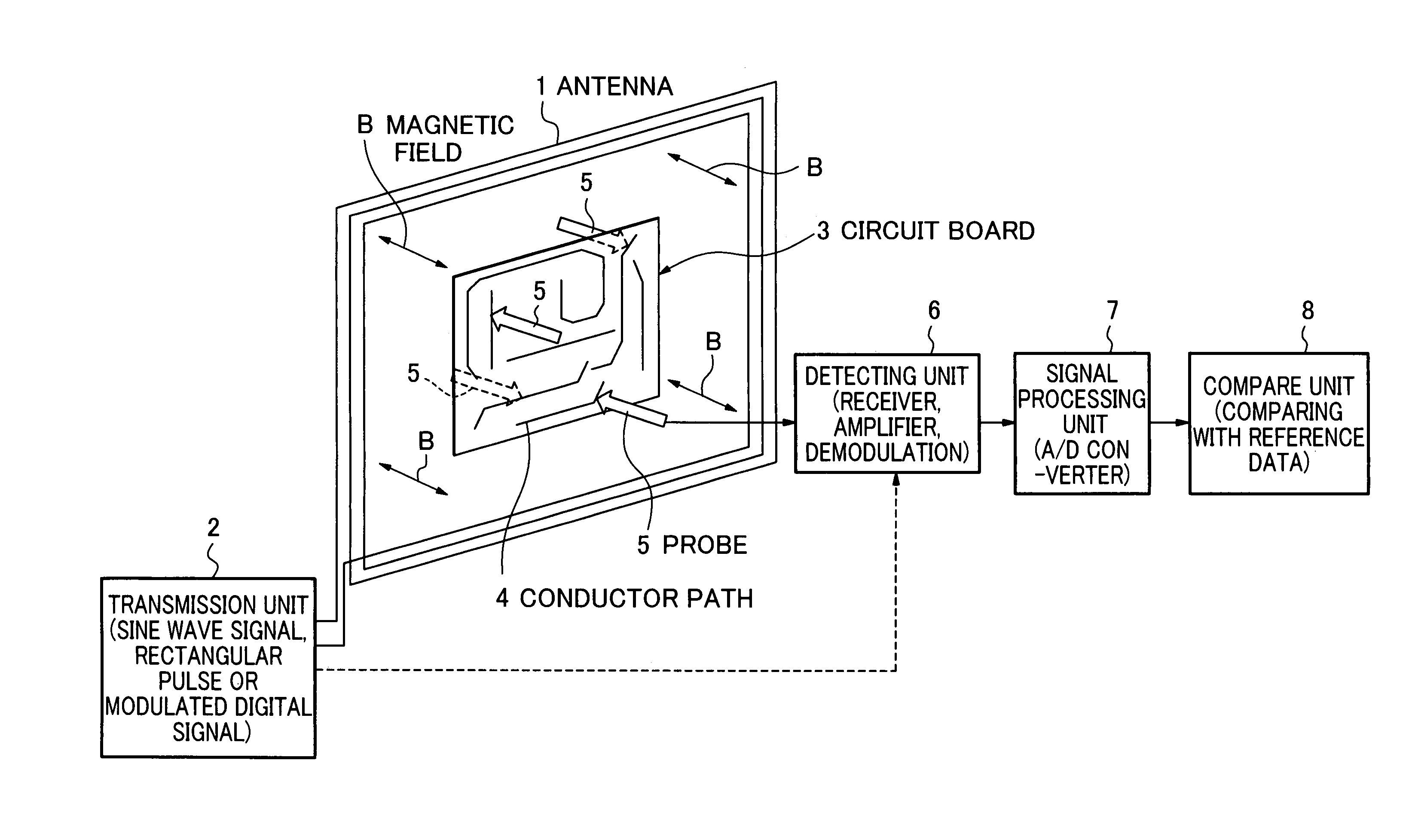
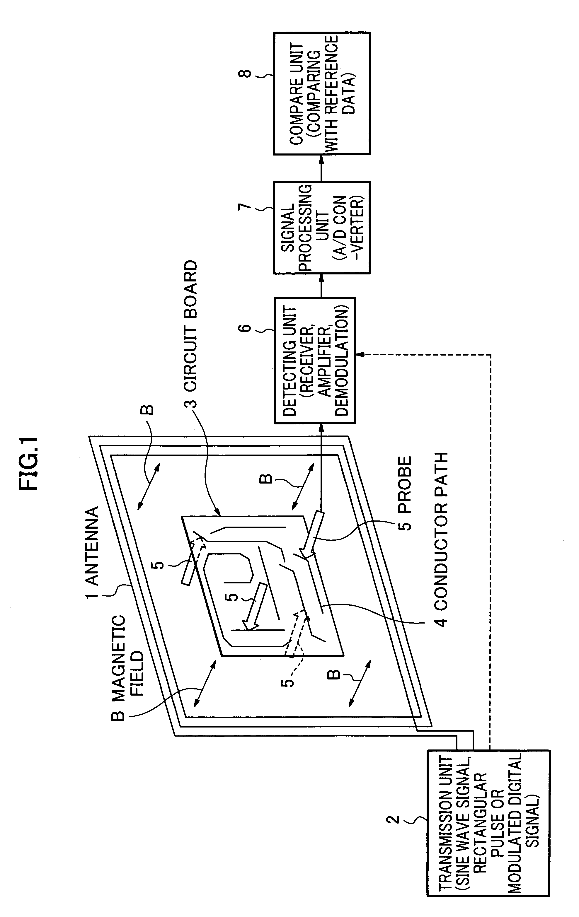
[0044]Apparatus according to one preferred embodiment of the present invention is schematically shown in FIG. 1. In this embodiment, the apparatus has an antenna 1 of rectangular loop coil for transmitting electromagnetic (radio) wave signal, that is, radio frequency signal, to a circuit board 3 under test. The rectangular loop coil antenna 1 is positioned so that its axis is parallel with a horizontal floor (not shown) on which the apparatus is installed. Therefore, the plane on which rectangular loop coil antenna 1 is positioned is perpendicular to the horizontal floor (not shown) on which the apparatus is installed. In alternative embodiments, circular loop coil, polygonal loop coil or any other antenna can be used as an antenna 1. The antenna 1 is connected to a transmission unit 2. The transmission unit 2 can send to the antenna 1 electromagnetic (radio) wave signal, that is, radio frequency signal, which includes any signal selected from a group comprising sine wave signal, bu...


PUM


Abstract

The invention provides a method of apparatus for testing circuit boards which does not require any inner wide power plane so as to detect an open circuit defect and / or a short circuit defect in a conductor path network formed in the circuit board quickly and accurately. An apparatus for testing a circuit board according to the present invention includes a transmission unit (2) for transmitting electromagnetic (radio) wave signal by way of an antenna (1) to a circuit board (3) to be tested, a detecting unit (3) for detecting signal received by a conductor path (4) of the circuit board (3) by using the conductor path (4) as a receiving antenna, and compare unit (8) for determining whether or not there is an open circuit defect or a short circuit defect in the conductor path (4) by comparing the detected signal with reference data of corresponding to a conductor path not including any defect.

Description

FIELD OF THE INVENTION[0001]This invention relates to a method and apparatus for testing circuit boards, and more particularly, to a method and apparatus for testing the integrity of electrical interconnections formed with conductor path networks of rigid or flexible circuit boards by using electromagnetic (radio) wave signal, that is, radio frequency (RF) signal.BACKGROUND OF THE INVENTION[0002]Rigid or flexible circuit boards are used for mounting and interconnecting electronic components in most electronic equipment. Typically, circuit boards have a plurality of laminated dielectric layers and a plurality of electrical interconnections formed with conductor path networks between or on the dielectric layers. It is necessary to test the integrity of electrical interconnections formed with conductor path networks in circuit boards before shipment so as to ensure the quality of circuit boards. The integrity of electrical interconnections formed with the conductor path networks in cir...

Claims


Application Information

Patent Timeline
Patent Type & Authority Patents(United States)
IPC IPC(8): G01R31/00
CPCG01R31/2806
Inventor HIDEHIRA, YORIO
Owner MICROCRAFT
Why Eureka
Try Eureka