Chip level hermetic and biocompatible electronics package using SOI wafers

a technology of biocompatible electronics and chips, applied in the direction of electrical equipment, semiconductor devices, semiconductor/solid-state device details, etc., can solve the problems of destroying devices, adding costs, and typically three-dimensional processes

Inactive Publication Date: 2007-03-13
SECOND SIGHT MEDICAL PRODS +1
View PDF14 Cites 89 Cited by
  • Summary
  • Abstract
  • Description
  • Claims
  • Application Information

AI Technical Summary

Problems solved by technology

The main drawback to thin film packaging of electronic circuits that are implanted in living tissue is that the process is typically three-dimensional since the entire IC needs to be packaged (encapsulated in a thin film).
This results in long deposition times that add cost and that could exceed the thermal budget of the electronic circuits, thereby destroying the device.

Method used


Image

  • Chip level hermetic and biocompatible electronics package using SOI wafers
  • Chip level hermetic and biocompatible electronics package using SOI wafers
  • Chip level hermetic and biocompatible electronics package using SOI wafers

Examples


Embodiment Construction

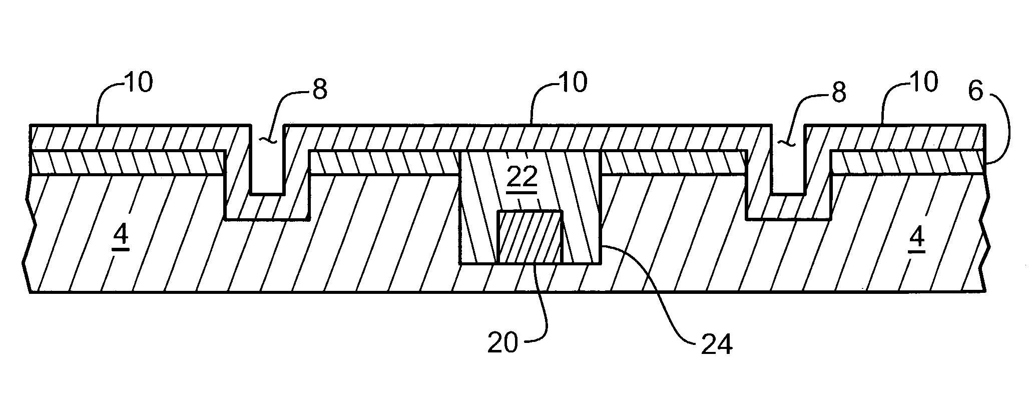
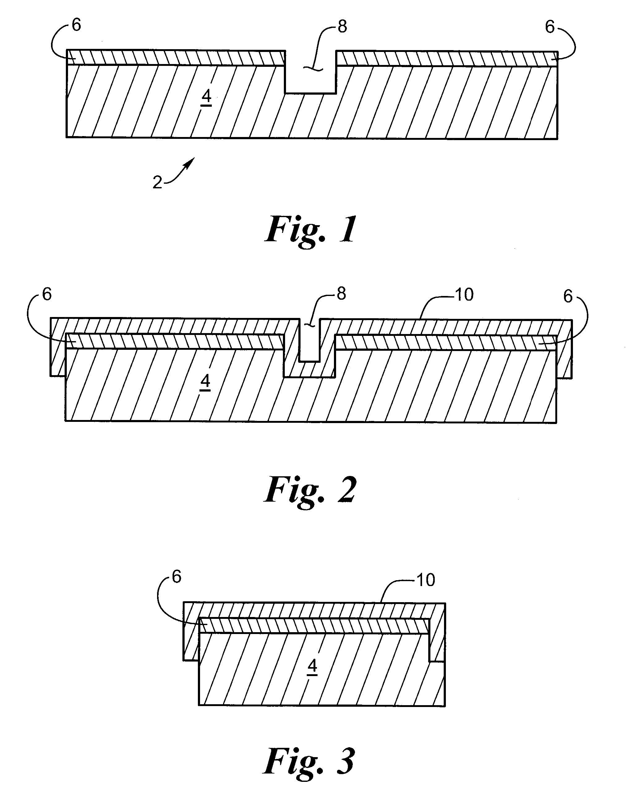
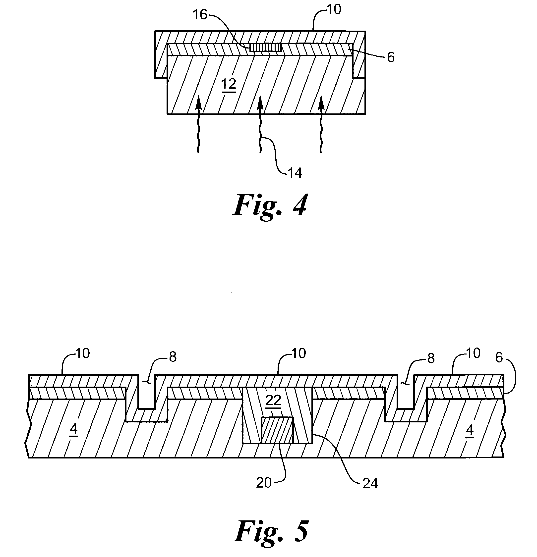
[0019]Starting with a base substrate wafer facilitates reducing process time. A silicon-on-insulator (SOI) wafer is used as the starting substrate as opposed to a standard silicon wafer. The invention is not limited to a silicon wafer, and it is envisioned that alternative semiconductors may be employed, such as gallium arsenide. In the case, where the integrated circuit (IC) is suitable for implantation in living tissue, a silicon-on-sapphire (SOS) or a silicon-on-diamond (SOD) wafer forms alternate embodiments, because the insulating layer is both biocompatible and bio-inert. A preferred embodiment is to the broader class of SOI wafers for electronic circuits for forming ICs for electronic circuits.

[0020]Using these wafers, the circuitry is designed using an electronics process that is known to one skilled in the art (e.g., 0.5 um CMOS) and this process is conducted to produce a wafer of functional die, such as ICs or chips). Typically, such wafers are post-processed, such as bein...


PUM


Abstract

The invention is directed to a hermetically packaged and implantable integrated circuit for electronics that is made by producing streets in silicon-on-insulator chips that are subsequently coated with a selected electrically insulating thin film prior to completing the dicing process to yield an individual chip. A thin-layered circuit may transmit light, allowing a photodetector to respond to transmitted light to stimulate a retina, for example. Discrete electronic components may be placed in the three-dimensional street area of the integrated circuit package, yielding a completely integrated hermetic package that is implantable in living tissue.

Description

CROSS REFERENCE TO RELATED APPLICATION[0001]This application claims the benefit of U.S. Provisional Application No. 60 / 440,806, “Chip Level Hermetic and Biocompatible Electronics Package Using SQI Wafers”, filed Jan. 17, 2003 the disclosure of which is incorporated herein by reference.FIELD OF THE INVENTION[0002]This invention relates to a hermetic integrated circuit and a method of making an integrated electronic circuit by utilizing silicon-on-insulator (SOI) techniques.BACKGROUND OF THE INVENTION[0003]This invention relates to electrically insulating thin film processes that are hermetic and that are used to encapsulate integrated circuits (ICs) for the purpose of forming a protective package for an electronic circuit, where the ICs are applicable to devices that are implanted in living tissue, such as neural prostheses or retinal electrode arrays. The package may have electrical feedthroughs to connect electrically to the outside environment. The electric circuit may interface w...

Claims


Application Information

Patent Timeline
Patent Type & Authority Patents(United States)
IPC IPC(8): H01L23/58H01L21/762H01L21/84H01L27/01H01L27/12
CPCH01L21/76251H01L27/1203H01L21/84
Inventor MECH, BRIAN V.GREENBERG, ROBERT J.DELMAIN, GREGORY J.
Owner SECOND SIGHT MEDICAL PRODS
Why Eureka
Try Eureka