
Display device and method of driving the same

a display device and display device technology, applied in the direction of instruments, computing, electric digital data processing, etc., can solve the problems of not yet difficult for the conventional active matrix liquid crystal display device to reproduce images with high quality similar to that of crts, and difficulty in achieving image quality comparable for current passive matrix liquid crystal display devices. , to achieve the effect of improving the horizontal resolution of an active improving the image quality of a passive matrix liquid crystal display devi

Inactive Publication Date: 2007-03-13
SEMICON ENERGY LAB CO LTD
View PDF47 Cites 23 Cited by
  • Summary
  • Abstract
  • Description
  • Claims
  • Application Information

AI Technical Summary

Benefits of technology

[0031]In accordance with a fourth aspect of the present invention, in the method of driving a semiconductor display device, the modulated clock signal may be obtained by shifting a frequency of the reference clock signal on the basis of a Gaussian histogram.
[0032]In accordance with a fifth aspect of the present invention, in the method of driving a semiconductor display device, the modulated clock signal may be obtained by randomly shifting a frequency of the reference clock signal.
[0033]In accordance with a sixth aspect of the present invention, in the method of driving a semiconductor display device, the modulated clock signal may be obtained by shifting a frequency of the reference clock signal in the form of a sine wave.
[0044]In accordance with an eleventh aspect of the present invention, there is provided a semiconductor display device comprising a passive matrix circuit, wherein an image signal sampled on the basis of a modulated clock signal obtained by frequency modulating a reference clock signal is inputted to a signal electrode of the passive matrix circuit, and a modulated clock signal which differs from the modulated clock signal in quantity of frequency shifting or method of frequency modulation is inputted to a scanning electrode of the passive matrix circuit.
[0047]In accordance with a fourteenth aspect of the present invention, in the semiconductor display device, the modulated clock signal may be obtained by shifting a frequency of the reference clock signal in the form of a sine wave.

Problems solved by technology

However, if CRTs are used, problems such as power consumption, volume and weight become serious according to the requirements for the sizes and resolutions of screens.
As described above, the conventional active matrix liquid crystal display devices are lower in horizontal resolution than CRTs which conform to the same standards, so that it is difficult for the conventional active matrix liquid crystal display devices to reproduce images with high quality similar to that of CRTs.
However, the current passive matrix liquid crystal display devices have not yet achieved image quality comparable to that of active matrix liquid crystal display devices.

Method used


Image

  • Display device and method of driving the same
  • Display device and method of driving the same
  • Display device and method of driving the same

Examples


embodiment 1

[0093]In the description of the present embodiment, reference will be made to an active matrix liquid crystal display device as one example of a semiconductor display device for which a driving method of a semiconductor display device according to the present invention can be used.

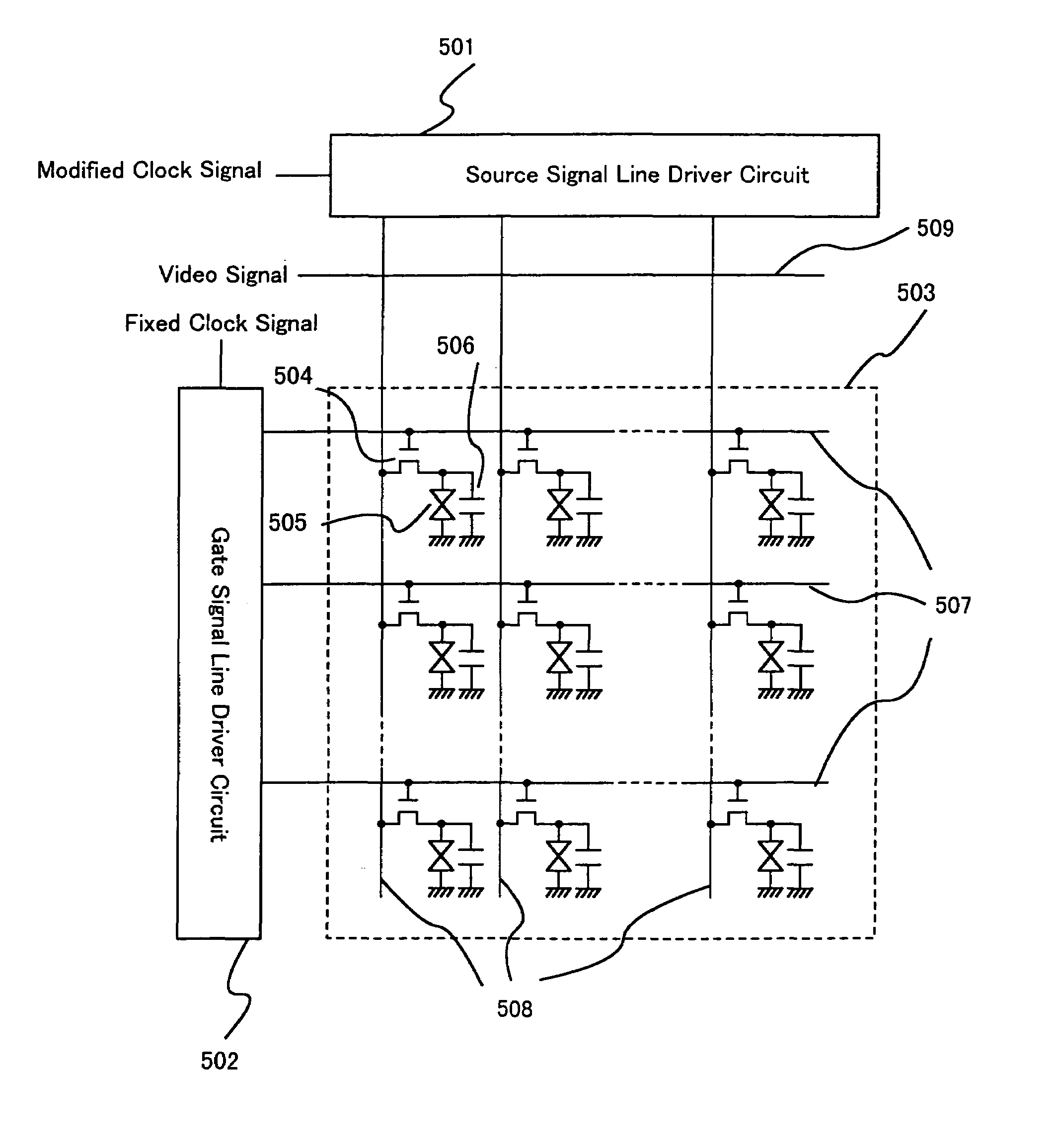
[0094]Reference will be made to FIG. 5. FIG. 5 shows a schematic block diagram of the active matrix liquid crystal display device of the present embodiment. Reference numeral 501 denotes a source signal line-side driving circuit to which a modulated clock signal, a start pulse and the like are to be inputted. Reference numeral 502 denotes a gate signal line-side driving circuit to which a fixed clock, a start pulse and the like are to be inputted. The term “fixed clock” used here in means a clock signal which operates at a constant frequency on the basis of a reference clock signal. Reference numeral 503 denotes an active matrix circuit which has pixels arranged in a matrix form so that one pixel is dispos...

embodiment 2

[0147]In the description of the present embodiment, reference will be made to an example in which inverted stagger TFTs are used for an active matrix liquid crystal display device which can realize the driving method according to the present invention.

[0148]Reference will be made to FIG. 13. FIG. 13 shows a cross-sectional view of an inverted stagger N-channel TFT which constitutes part of the active matrix liquid crystal display device of the present embodiment. Needless to say, although FIG. 13 shows only one N-channel TFT, it is possible to construct a CMOS circuit with a P-channel TFT and an N-channel TFT as in the case of Embodiment 1. In addition, it goes without saying that each pixel TFT can be formed to have a similar construction.

[0149]Reference numeral 1301 denotes a substrate, and a substrate such as that described above in connection with Embodiment 1 is used as the substrate 1301. Reference numeral 1302 denotes a silicon oxide film. Reference numeral 1303 denotes a gat...

embodiment 3

[0150]In the description of the present embodiment, reference will be made to an example in which an active matrix liquid crystal display device is made of inverted stagger TFTs which differ in construction from those of Embodiment 3.

[0151]Reference will be made to FIG. 14. FIG. 14 shows a cross-sectional view of an inverted stagger N-channel TFT which constitutes part of the active matrix liquid crystal display device of the present embodiment. Needless to say, although FIG. 14 shows only one N-channel TFT, it is possible to construct a CMOS circuit with a P-channel TFT and an N-channel TFT as in the case of Embodiment 1. In addition, it goes without saying that each pixel TFT can be formed to have a similar construction.

[0152]Reference numeral 1401 denotes a substrate, and a substrate such as that described above in connection with Embodiment 1 is used as the substrate 1401. Reference numeral 1402 denotes a silicon oxide film. Reference numeral 1403 denotes a gate electrode. Refer...


PUM


Abstract

The present invention is intended to achieve an improvement in the horizontal resolution of an active matrix semiconductor display device. In accordance with the present invention, by supplying a modulated clock signal obtained by frequency modulating a reference clock signal at a constant period to a driving circuit of an active matrix semiconductor display device or to a driving circuit of a passive matrix semiconductor display device, signal information (the presence or absence of an edge, the extent of nearness) relative to the vicinity of the sampling of video signals (image signals) sampled on the basis of this modulated clock signal can be written to the corresponding pixels of the semiconductor display device as shading information. The driving method of the present invention makes use of a phenomenon which apparently makes the resolution of an image display higher owing to the shading information (visual Mach phenomenon and Craik-O'Brien phenomenon).

Description

BACKGROUND OF THE INVENTION[0001]1. Field of the Invention[0002]The present invention relates to a method of driving a display device and to a display device using the driving method, and more particularly to a method of driving an active matrix semiconductor display device having thin-film transistors (TFTs) fabricated over an insulating substrate. In addition, the present invention relates to an active matrix semiconductor display device using the driving method, and more particularly to an active matrix liquid crystal display device which is one type of active matrix semiconductor display device. The present invention is also applicable to a passive matrix type display device.[0003]2. Description of Related Art[0004]The art of forming semiconductor thin films over an inexpensive glass substrate and fabricating thin-film transistors (TFTs) has recently been making rapid progress. The reason for this is that a demand for active matrix liquid crystal display devices (liquid crystal ...

Claims


Application Information

Patent Timeline
IPC IPC(8): G09G5/00G09G3/20G09G3/36G09G5/18
CPCG09G3/3633G09G3/3688G09G3/3677G09G3/2018G09G3/3622G09G2340/0407G09G5/18G09G2310/0205G09G3/20
Inventor HIROKI, MASAAKI
Owner SEMICON ENERGY LAB CO LTD
Learn More