Wafer level package and fabrication method

a technology of wafers and packaging, applied in the direction of electrical equipment, semiconductor devices, semiconductor/solid-state device details, etc., can solve the problems of placing a fundamental restriction on the minimum size of the electronic component package, large impedance associated with the bond wire, and flip chip bumps between the bond pads of the integrated circuit chip and the traces on the substrate, so as to minimize impedance, simplify manufacturing, and maximize the reliability of the electrical connection

Inactive Publication Date: 2007-03-20
AMKOR TECH SINGAPORE HLDG PTE LTD
View PDF378 Cites 126 Cited by
  • Summary
  • Abstract
  • Description
  • Claims
  • Application Information

AI Technical Summary

Benefits of technology

[0011]Thus, in accordance with this embodiment of the present invention, the bond pads are directly connected to the corresponding first vias. Stated another way, the bond pads are electrically connected to the corresponding first vias without the use of a solder, e.g., without the use of flip chip bumps, and without the need to form a solder wetting layer, e.g., a nickel / gold layer, on the bond pads. This maximizes the reliability of the electrical connection between the first vias and the bond pads, while at the same time minimizes impedance.
[0012]Further, since the dielectric strip is directly attached to the electronic component and the bond pads are directly connected to the corresponding first vias, the use of an underfill material is obviated. This simplifies manufacturing, enhances reliability, and thus reduces cost.

Problems solved by technology

However, in the wirebond configuration described above, the traces of the substrate were fanned out around the integrated circuit chip, which placed a fundamental restriction on the minimum electronic component package size.
Further, a large impedance was associated with the bond wires.
However, the flip chip bumps between the bond pads of the integrated circuit chip and the traces on the substrate were subject to significant stress, e.g., due to differential thermal expansion between the integrated circuit chip and the substrate.
Thus, failure of the flip chip bumps often occurred which decreased yield and thus increased the cost of the electronic component package.
However, the application of the underfill material required an additional manufacturing step, which increased the cost of the electronic component package.

Method used


Image

  • Wafer level package and fabrication method
  • Wafer level package and fabrication method
  • Wafer level package and fabrication method

Examples


Embodiment Construction

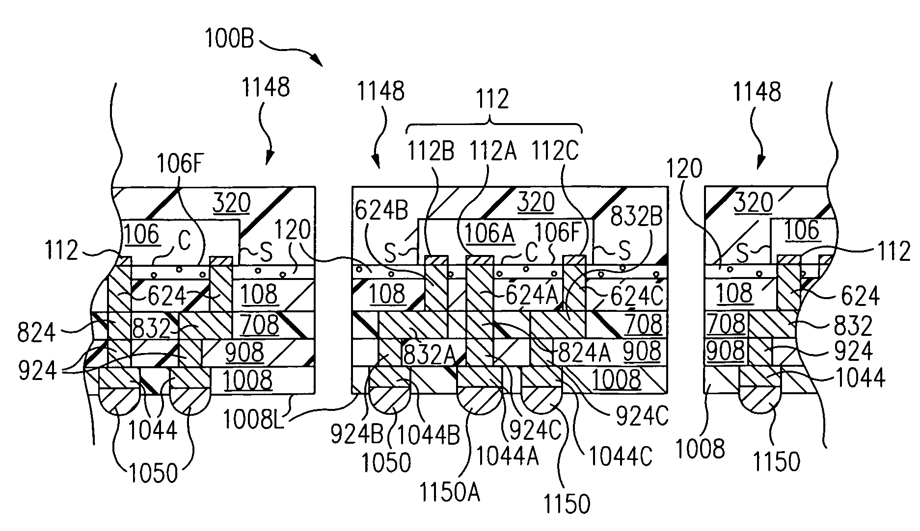
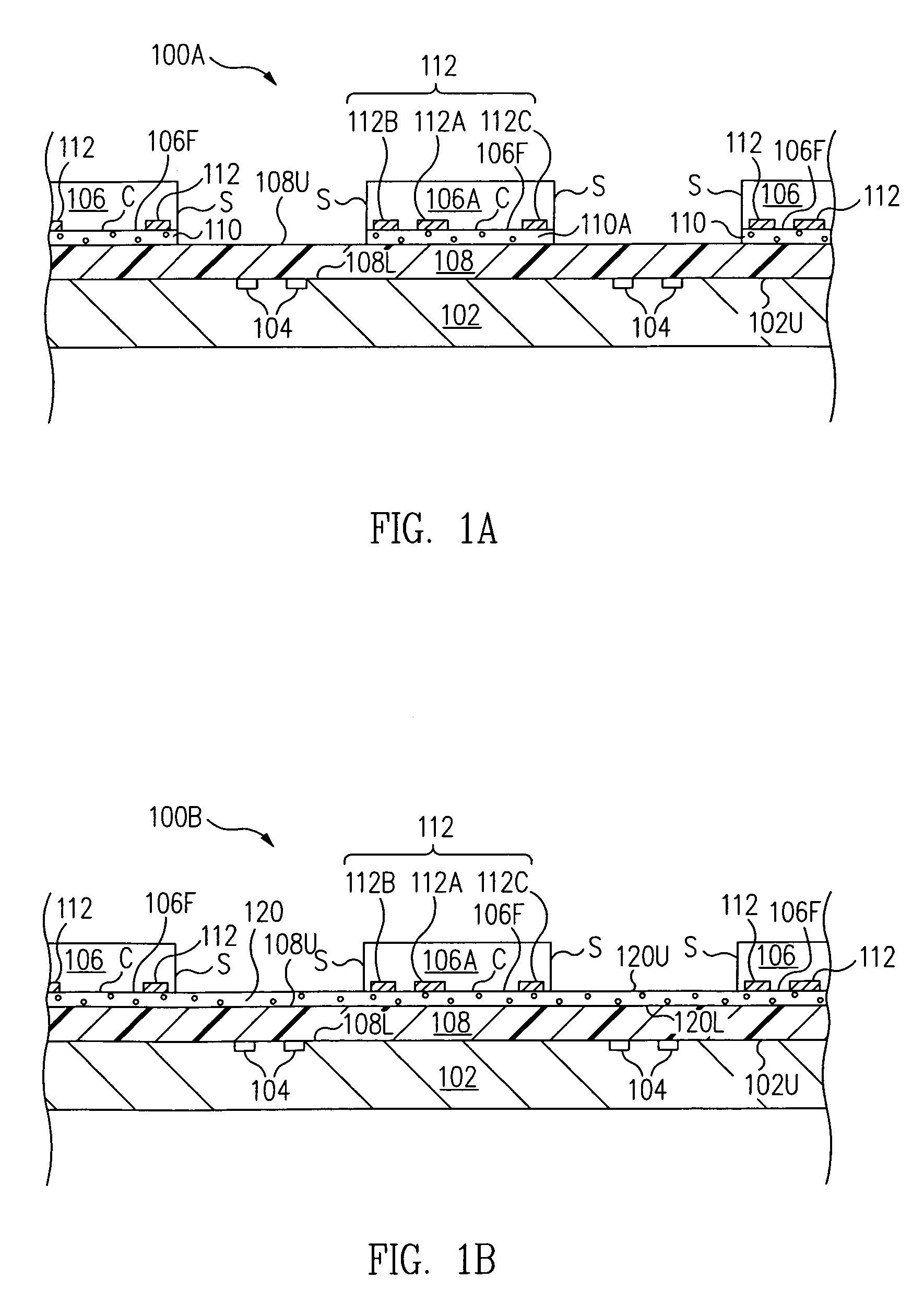
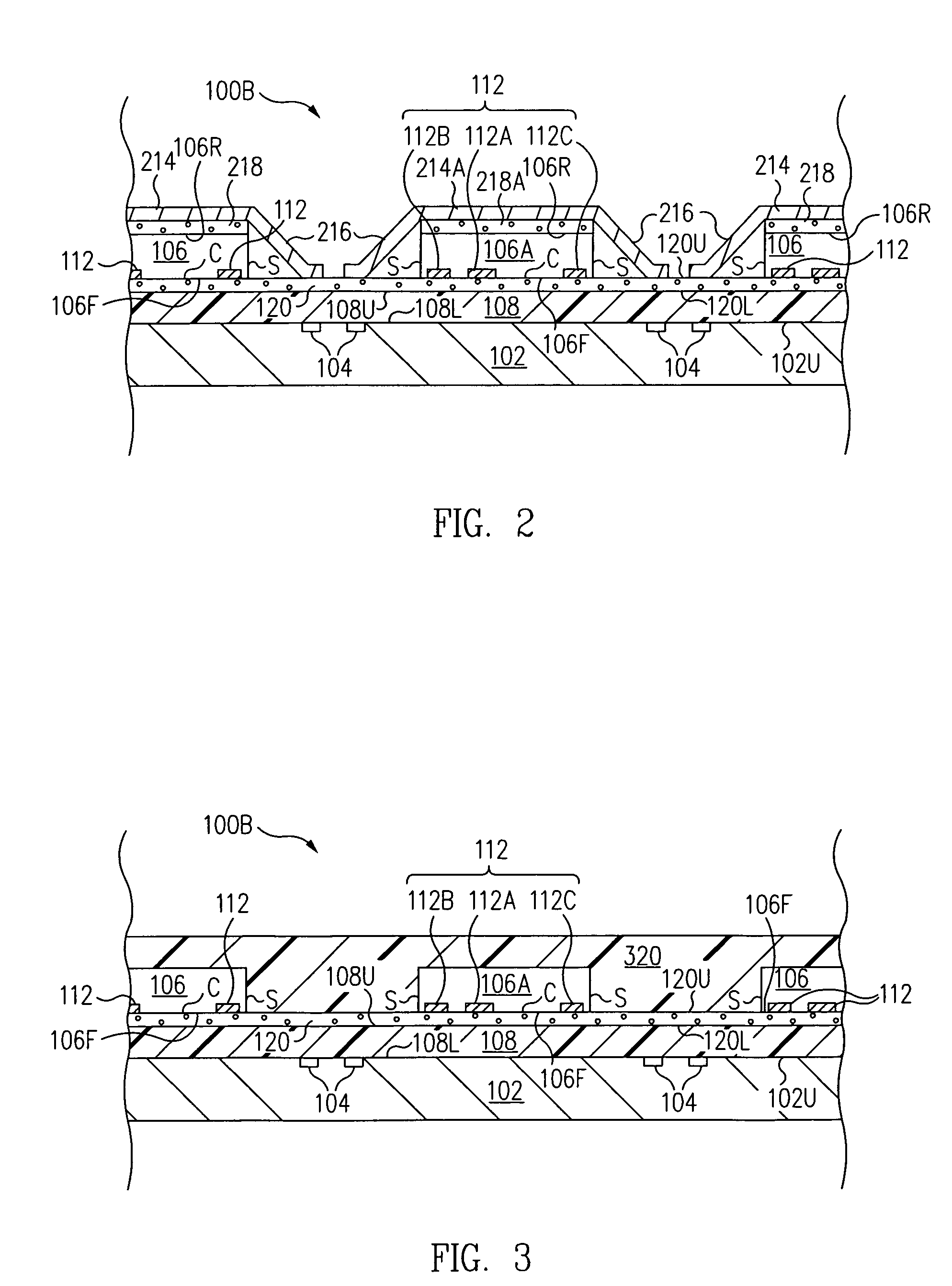
[0020]In accordance with one embodiment of the present invention, a method of forming an electronic component package includes coupling first surfaces 106F of electronic components 106 to a first surface 108U of a dielectric strip 108 with adhesives 110 or 120 (FIGS. 1A and 1B), electronic-components 106 having bond pads 112 on first surfaces 106F; forming via apertures 522 through dielectric strip 108 to expose bond pads 112 (FIG. 5); and filling via apertures 522 with an electrically conductive material to form vias 624 electrically coupled to bond pads 112 (FIG. 6).

[0021]Thus, in accordance with this embodiment of the present invention, bond pads 112 are directly connected to corresponding vias 624. Stated another way, bond pads 112 are electrically connected to corresponding vias 624 without the use of a solder, e.g., without the use of flip chip bumps, and without the need to form a solder wetting layer, e.g., a nickel / gold layer, on bond pads 112. This maximizes the reliabilit...


PUM


Abstract

A method of forming an electronic component package includes coupling a first surface of an electronic component to a first surface of a first dielectric strip, the electronic component comprising bond pads on the first surface; forming first via apertures through the first dielectric strip to expose the bond pads; and filling the first via apertures with an electrically conductive material to form first vias electrically coupled to the bond pads. The bond pads are directly connected to the corresponding first vias without the use of a solder and without the need to form a solder wetting layer on the bond pads.

Description

RELATED APPLICATIONS [0001]This application is a continuation of Huemoeller et al., U.S. patent application Ser. No. 10 / 291,050, filed on Nov. 8, 2002, entitled “WAFER LEVEL PACKAGE AND FABRICATION METHOD”, now U.S. Pat. No. 6,905,914, issued Jun. 14, 2005, which is herein incorporated by reference in its entirety.BACKGROUND OF THE INVENTION[0002]1. Field of the Invention[0003]The present invention relates generally to the packaging of electronic components. More particularly, the present invention relates to a wafer level package and method of fabricating the same.[0004]2. Description of the Related Art[0005]One form of an electronic component package included an electronic component such as an integrated circuit chip mounted to a substrate. For example, in a wirebond configuration, the rear surface of the integrated circuit chip was mounted to the substrate, e.g., with an adhesive. Bond wires were used to form the electrical interconnections between the bond pads on the front surf...

Claims


Application Information

Patent Timeline
Patent Type & Authority Patents(United States)
IPC IPC(8): H01L21/00H01L21/60H01L21/68H01L23/538
CPCH01L21/6835H01L23/481H01L24/19H01L24/97H01L23/5389H01L2221/68345H01L2224/04105H01L2224/20H01L2224/83192H01L2224/92144H01L2224/97H01L2924/01013H01L2924/01029H01L2924/01047H01L2924/01075H01L2924/01078H01L2924/01079H01L2924/01082H01L2924/01322H01L2924/14H01L2924/15311H01L2924/3011H01L2924/014H01L2924/01033H01L2924/01023H01L2924/01006H01L2924/01019H01L2224/82H01L2224/12105H01L2224/83132H01L2224/8314H01L21/56H01L21/568H01L21/76802H01L21/76877H01L21/82H01L21/561H01L21/78H01L24/96H01L23/3157
Inventor HUEMOELLER, RONALD PATRICKRUSLI, SUKIANTORAZU, DAVID
Owner AMKOR TECH SINGAPORE HLDG PTE LTD
Why Eureka
Try Eureka