Intermediate chip module, semiconductor device, circuit board, and electronic device

a technology of semiconductor devices and chips, applied in semiconductor devices, semiconductor/solid-state device details, electrical apparatus, etc., can solve the problems of difficult connection between the terminal and the outside terminal, limited space for mounting such electronic components, and inability to achieve the redistribution layer only by this technique, etc., to achieve flexibly packaged and enhanced density

Active Publication Date: 2007-03-20
ADVANCED INTERCONNECT SYST LTD
View PDF15 Cites 375 Cited by
  • Summary
  • Abstract
  • Description
  • Claims
  • Application Information

AI Technical Summary

Benefits of technology

[0010]A first aspect of the present invention was conceived in view of the above-mentioned background, and an object thereof is to provide an intermediate chip for electrically connecting semiconductor chips, and a semiconductor device, a circuit board and an electronic device having such an intermediate chip, as a three-dimensional chip stacking technique which allows a redistribution layer without affecting the manufacturing process of the semiconductor chips.

Problems solved by technology

Spaces for mounting such electronic components are also limited.
In the three-dimensional chip stacking technique, increasing density of semiconductor chips has reduced pitches between terminals, making connection between the terminals and outside terminal difficult.
However, since all junctions of semiconductor chips are provided at the same position in the technique disclosed in JP 2002-170919, a redistribution layer cannot be achieved solely by this technique.
However, since an additional wiring is added to a semiconductor circuit, the manufacturing process becomes complex, and the yield is reduced.

Method used


Image

  • Intermediate chip module, semiconductor device, circuit board, and electronic device
  • Intermediate chip module, semiconductor device, circuit board, and electronic device
  • Intermediate chip module, semiconductor device, circuit board, and electronic device

Examples


second embodiment

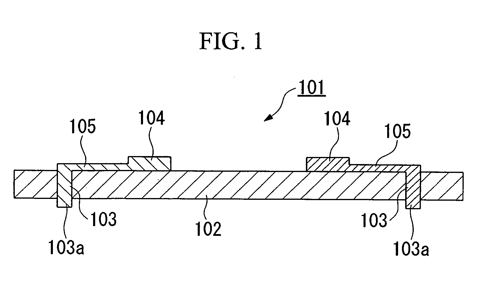
[0162]An embodiment of an intermediate chip module according to the second aspect of the present invention will be explained based on a manufacturing method thereof. First, manufacturing steps for manufacturing a semiconductor chip (semiconductor wafer) which is included an intermediate chip module will be explained with reference to schematic diagrams of FIGS. 10A–C.

[0163]As shown in FIG. 10A, a silicon substrate (wafer) 210, a base material for forming a semiconductor chip, is provided. Although various components and circuits, such as transistors and memory elements, are formed on the front side (active side) of the silicon substrate 210, they are not shown in this figure.

[0164]Next, openings are formed at predetermined positions on the front side of the silicon substrate 210. Conductive material, e.g., copper, is filled into the openings and electrodes 243 which will be formed into trans-substrate conductive plugs in a later step are formed, as shown in FIG. 10B. The silicon sub...


PUM


Abstract

An intermediate chip for electrically connecting semiconductor chips includes: a substrate having a first side and a second side; a trans-substrate conductive plug which projects to the first side of the substrate; a post electrode which is displaced from the trans-substrate conductive plug in plan view on the second side of the substrate; and wiring which is disposed in or on the substrate for coupling the trans-substrate conductive plug and the post electrode.

Description

[0001]Priority is claimed on Japanese Patent Application No. 2003-335675 filed Sep. 26, 2003, and Japanese Patent Application No. 2003-386512, filed Nov. 17, 2003, the contents of which are incorporated herein by reference.BACKGROUND OF THE INVENTION[0002]1. Field of the Invention[0003]The present invention relates to an intermediate chip for electrically connecting semiconductor chips, and relates to a semiconductor device, a circuit board, and an electronic device having semiconductor chips electrically connected by means of such an intermediate chip. The present invention also relates to an intermediate chip module, a semiconductor device, a circuit board, and an electronic device.[0004]2. Description of Related Art[0005]Currently, efforts are being made to reduce the size of electronic components (e.g., semiconductor chips) used in mobile electronic devices, such as portable telephones, notebook personal computers, PDAs (Personal Data Assistants) in general, so that the size and...

Claims


Application Information

Patent Timeline
Patent Type & Authority Patents(United States)
IPC IPC(8): H01L23/02H01L21/768H01L23/00H01L23/12H01L23/48H01L23/62H01L25/00H01L25/065
CPCH01L21/76898H01L25/0657H01L25/50H01L23/481H01L24/97H01L24/94H01L2224/97H01L2225/06513H01L2225/06517H01L2225/06527H01L2225/06541H01L2225/06572H01L2924/09701H01L2924/19011H01L2224/94H01L2224/81H01L2224/05548H01L2224/13009H01L2924/14H01L2924/15787H01L2924/00H01L25/065
Inventor MATSUI, KUNIYASU
Owner ADVANCED INTERCONNECT SYST LTD
Why Eureka
Try Eureka