High frequency transmission line and high frequency board

a high frequency transmission line and high frequency board technology, applied in the direction of waveguides, waveguide type devices, high frequency circuit adaptations, etc., can solve the problems of not being able to apply public knowledge methods, impedance deviation cannot be neglected, and known connection structures cannot be directly applied to the connection portion between two high frequency transmission lines. , to achieve the effect of superior signal passing characteristic and reducing signal reflection

Active Publication Date: 2007-03-20
TDK CORPARATION
View PDF17 Cites 23 Cited by
  • Summary
  • Abstract
  • Description
  • Claims
  • Application Information

AI Technical Summary

Benefits of technology

[0012]The present invention has been made to solve the above-explained problems of the conventional techniques, and has an object to provide a high frequency transmission line and a high frequency board using this high frequency transmission line. That is, in such a case that a high frequency line is constructed by connecting different high frequency transmission lines to each other, the high frequency transmission line is capable of reducing signal reflections occurred at a connection portion between these different high frequency transmission lines, and thus owns a superior signal passing characteristic.

Problems solved by technology

However, in such a connection structure, signal reflections occurred at the connection portion are increased with respect to the above-described high frequency signals, so that the high frequency signals can hardly pass through this connection portion.
However, this known connection structure cannot be directly applied to a connection portion between two high frequency transmission lines having different structures from each other.
As previously explained, these public knowledge methods cannot be applied to such a case that the signal lines are arranged in different dielectric substrate layers.
However, when a frequency of a transmission signal is high, this impedance deviation cannot be neglected.
As a result, an impedance matching condition can be no longer established in the connection portion, and thus, reflections of transmission signals may occur, which may cause a signal passage characteristic to be deteriorated.

Method used


Image

  • High frequency transmission line and high frequency board
  • High frequency transmission line and high frequency board
  • High frequency transmission line and high frequency board

Examples


embodiment mode 1

(Embodiment Mode 1)

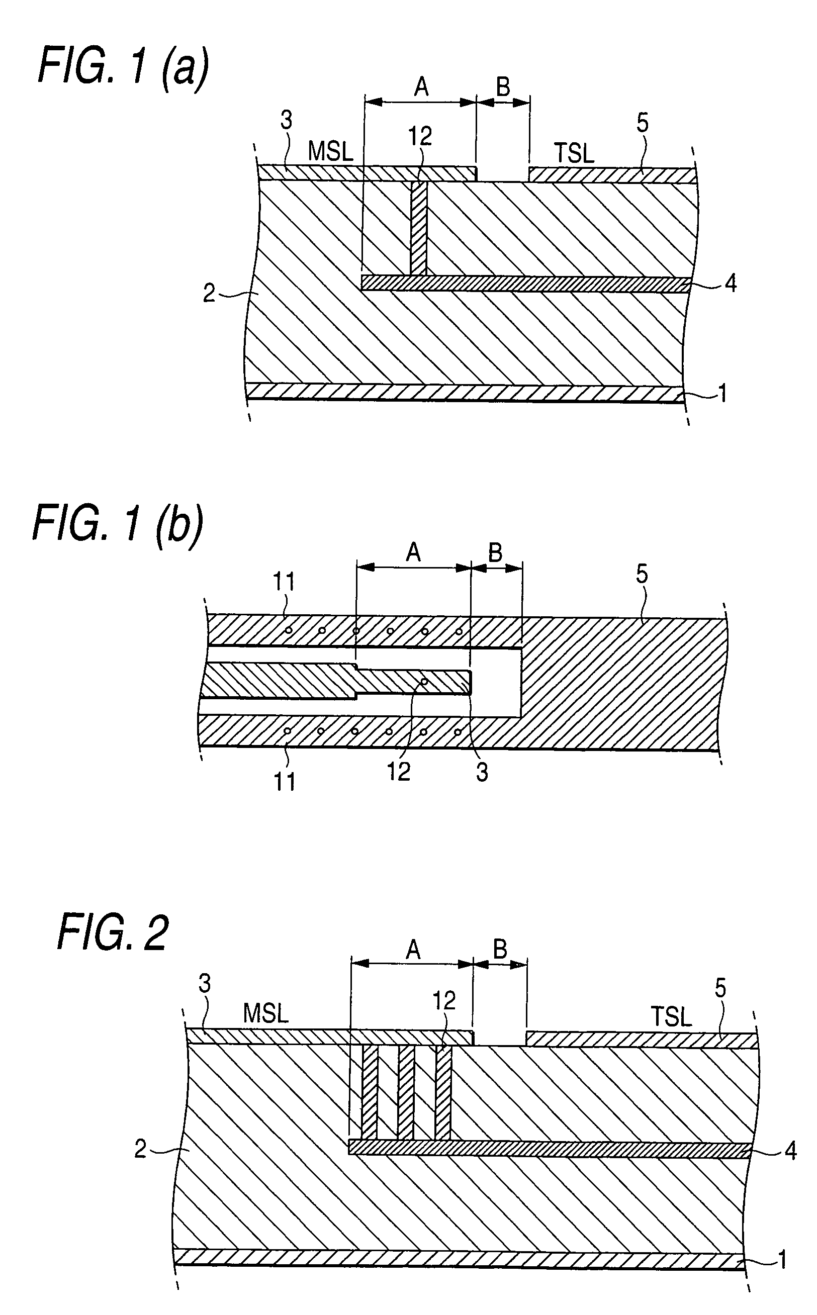
[0059]Next, a description is made of embodiment modes according to the present invention based upon drawings. FIG. 1 is a sectional view and a plane view, which represent a connection structure of a high frequency transmission line according to a first embodiment mode of the present invention. It should be noted that the same reference numerals shown in the prior art will be employed as those for indicating the same, or similar structural elements of FIG. 1.

[0060]As indicated in FIG. 1(a), in the high frequency transmission line according to this embodiment, while a dielectric substrate 2 is commonly used by a microstrip signal line (MSL) and a triplate signal line (TSL), a ground conductor 1 which is commonly used by both the microstrip line and the triplate line has been formed on a lower plane (namely, lower layer) of this dielectric substrate 2. On the other hand, a signal line 3 of the microstrip line has been formed on an upper plane (namely, upper layer) of...

embodiment mode 2

(Embodiment Mode 2)

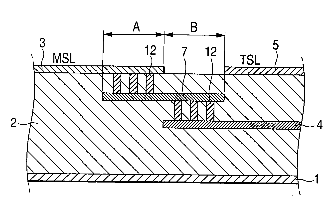
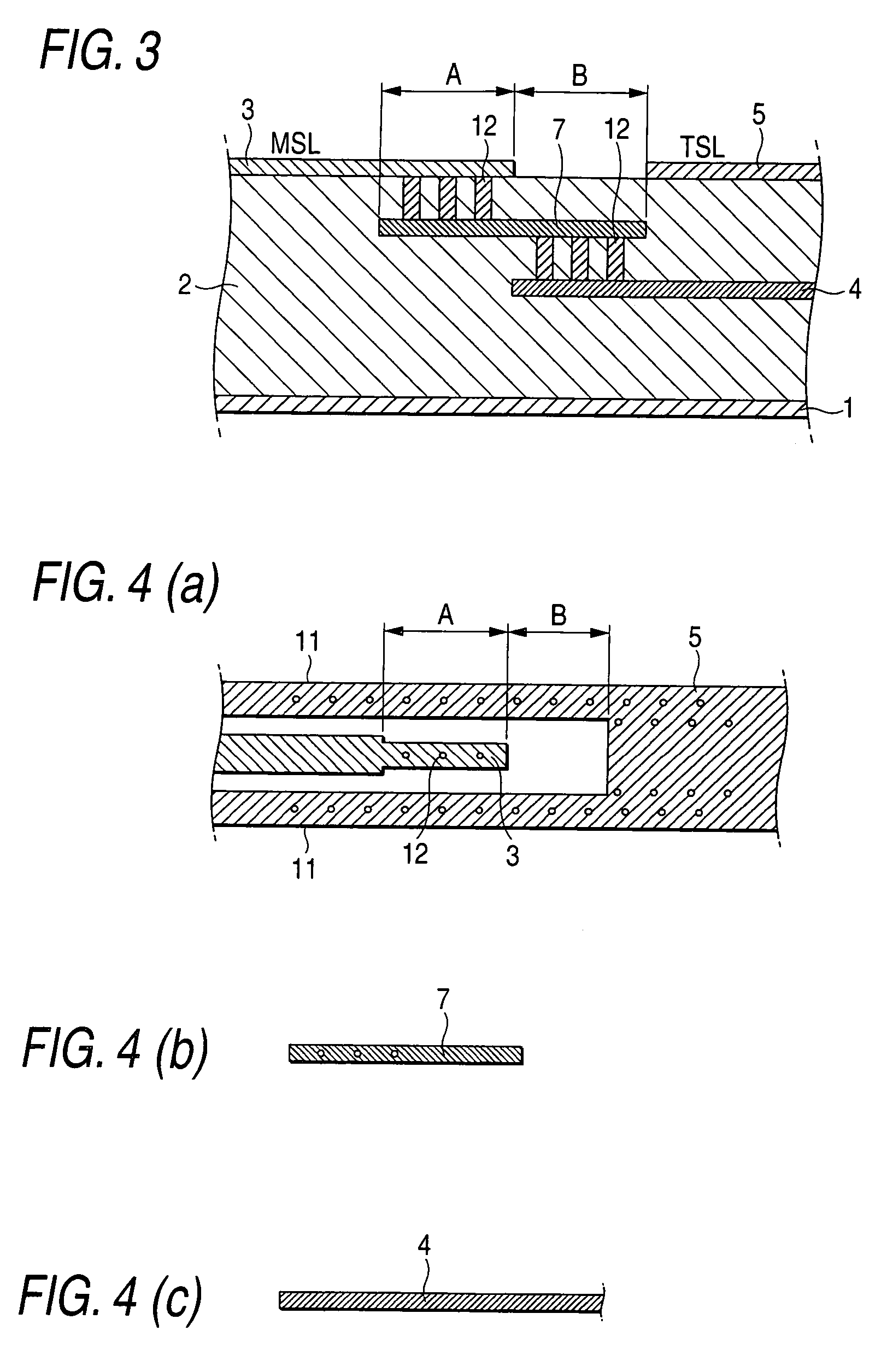
[0068]FIG. 2 is a sectional view for showing a connection structure of a high frequency transmission line according to a second embodiment mode of the present invention. It should be noted that the same reference numerals indicated in the first embodiment mode will be employed as those for representing the same, or similar structural elements of the second embodiment mode.

[0069]Similar to the first embodiment, in the high frequency transmission line of this second embodiment, a width of a signal line 3 of a microstrip line (MSL) is made narrow in an area “A.” However, this high frequency transmission line owns such a different point that the signal line 3 of the microstrip line is connected to a signal line 4 of a triplate line (TSL) by employing three pieces of via hole conductors 12, as compared with that of the first embodiment.

[0070]In accordance with this second embodiment, since these signal lines 3 and 4 are connected to each other by employing a plurality ...

embodiment mode 3

(Embodiment Mode 3)

[0074]FIG. 3 is a sectional view for showing a connection structure of a high frequency transmission line according to a third embodiment mode of the present invention. It should be noted that the same reference numerals indicated in the first embodiment mode will be employed as those for representing the same, or similar structural elements of the third embodiment mode.

[0075]Similar to the first embodiment, a ground conductor 1 is formed on a lower plane (namely, lower layer) of a dielectric substrate 2, a signal line 3 of a microstrip line (MSL) and a ground conductor 5 of a triplate line (TSL) are formed on an upper plane (namely, upper layer) of the dielectric substrate 2. Also, a signal line 4 of a triplate line is embedded in an inner portion (namely, inner layer) of the dielectric substrate 2 in such a manner that this signal line 4 is sandwiched by the ground conductors 1 and 5. It should also be noted that an edge portion of the triplate line 4 is elongat...


PUM


Abstract

Since a width of an edge portion of a signal line of a first high frequency transmission line is changed with respect to a width of another portion thereof, a deviation of impedances in a connection portion of the first and second high frequency transmission lines can be suppressed, so that signal reflections occurred in the connection portion can be lowered and a signal passing characteristic is improved.

Description

BACKGROUND OF THE INVENTION[0001]The present invention is related to a high frequency transmission line. More specifically, the present invention is directed to a high frequency transmission line which is fabricated by combining different high frequency transmission lines with each other, and also directed to a high frequency board on which these different high frequency transmission lines are wired.[0002]Conventionally, either microstrip lines or triplate lines are known as high frequency transmission lines for transmitting the high frequency signals. Generally speaking, as indicated in FIG. 14, a microstrip line is constituted by a dielectric substrate 2, a ground conductor (ground layer) 1, and a signal line (signal conductive line) 3. The ground conductor 1 has been formed on a lower plane (namely, lower layer) of this dielectric substrate 2. The signal line 3 has been formed on an upper plane (namely, upper layer) of this dielectric substrate 2. It should be noted that FIG. 14 ...

Claims


Application Information

Patent Timeline
Patent Type & Authority Patents(United States)
IPC IPC(8): H01P3/08H01P5/08H05K1/02H05K1/11
CPCH01P5/08H05K1/0251H05K1/0219H05K1/0222H05K2201/09845H05K1/115H05K2201/09618H05K2201/0979
Inventor SHIMODA, HIDEAKI
Owner TDK CORPARATION
Why Eureka
Try Eureka