Versatile system for wafer edge remediation

a technology of wafer edge and remediation system, which is applied in the direction of cleaning process and apparatus, cleaning process using liquids, chemistry apparatus and processes, etc., can solve the problems of increasing the number of physical aberrations in the structure of the wafer, affecting the production yield of the semiconductor, and causing significant damage to the entire wafer, so as to improve production yield, improve the effect of yield and safety, and improve the effect of production yield

Active Publication Date: 2007-03-27
TEXAS INSTR INC
View PDF17 Cites 4 Cited by
  • Summary
  • Abstract
  • Description
  • Claims
  • Application Information

AI Technical Summary

Benefits of technology

[0007]The present invention provides a versatile system for wafer edge remediation, providing thorough remediation of aberrations and improving production yields, in an easy, efficient and cost-effective manner. Specifically, the present invention provides a system that safely remediates peeling, blistering and other structural anomalies occurring along the outer perimeter of a semiconductor wafer—particularly along its edge—without significantly affecting active area on the wafer. The present invention provides apparatus, methods, and chemistries, readily adaptable to semiconductor manufacturing processes, that safely bathe the outer perimeter of a wafer with a solution that strips away undesired aberrations and to debris—salvaging a wafer that might have otherwise been scrapped. The present invention provides a backside cleaning process that employs a specialized chuck, an isolation barrier, and solutions for dissolving desired materials. The present invention thus efficiently reclaims wafers having edge—aberrations resulting in higher yields and fewer reliability problems when compared to previous methods.

Problems solved by technology

The increased packing density of the integrated circuit generates numerous challenges to the semiconductor manufacturing process.
The differing physical properties (e.g., coefficient of thermal expansion) of the varied material layers, when subjected to the repetitive stresses of the fabrication process, can cause a number of physical aberrations in the wafer structure.
Even the most minor physical aberrations in the structural integrity of one portion of a wafer can cause significant, and even catastrophic, damage to the entire wafer.
Often, such aberrations take the form of peeling or blistering of structures along the outer edge of the wafer.
Peeling or blistering of edge structures can directly damage the structure of devices fabricated near the outer perimeter of the wafer.
More commonly, however, peeling and blistering of edge structures results in a chaff of small, broken pieces of material and debris that can scatter across the wafer surface and throughout the downstream processes.
The propagation of this debris can cause direct damage (e.g., tears and pits) to device structures throughout the wafer.
The propagation of this debris can further cause indirect damage to device structures by blocking later etch and deposition processes.
Regardless of the mode of damage done, such edge aberrations have, in the past, usually resulted in a significant yield loss, as wafers exhibiting such aberrations were scrapped completely.
It appears that there have previously been no successful systems for remediating such aberrations.
Where each wafer contained hundreds, if not thousands, of individual devices, a significant and costly yield loss resulted.

Method used


Image

  • Versatile system for wafer edge remediation
  • Versatile system for wafer edge remediation
  • Versatile system for wafer edge remediation

Examples


Embodiment Construction

[0017]While the making and using of various embodiments of the present invention are discussed in detail below, it should be appreciated that the present invention provides many applicable inventive concepts, which can be embodied in a wide variety of specific contexts. The invention will now be described in conjunction with remediating edge aberrations from a semiconductor wafer. The specific embodiments discussed herein are merely illustrative of specific ways to make and use the invention and do not limit the scope of the invention.

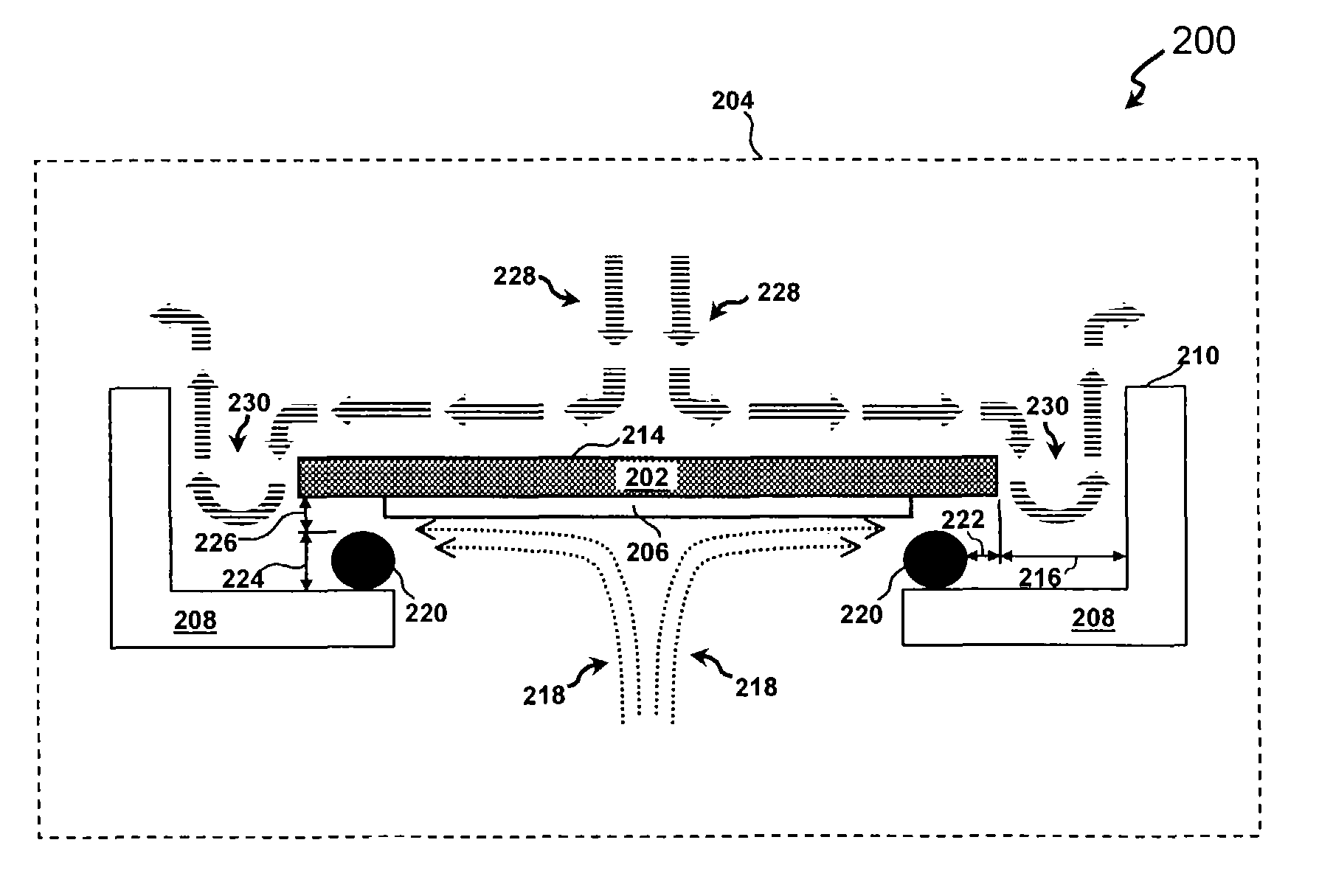
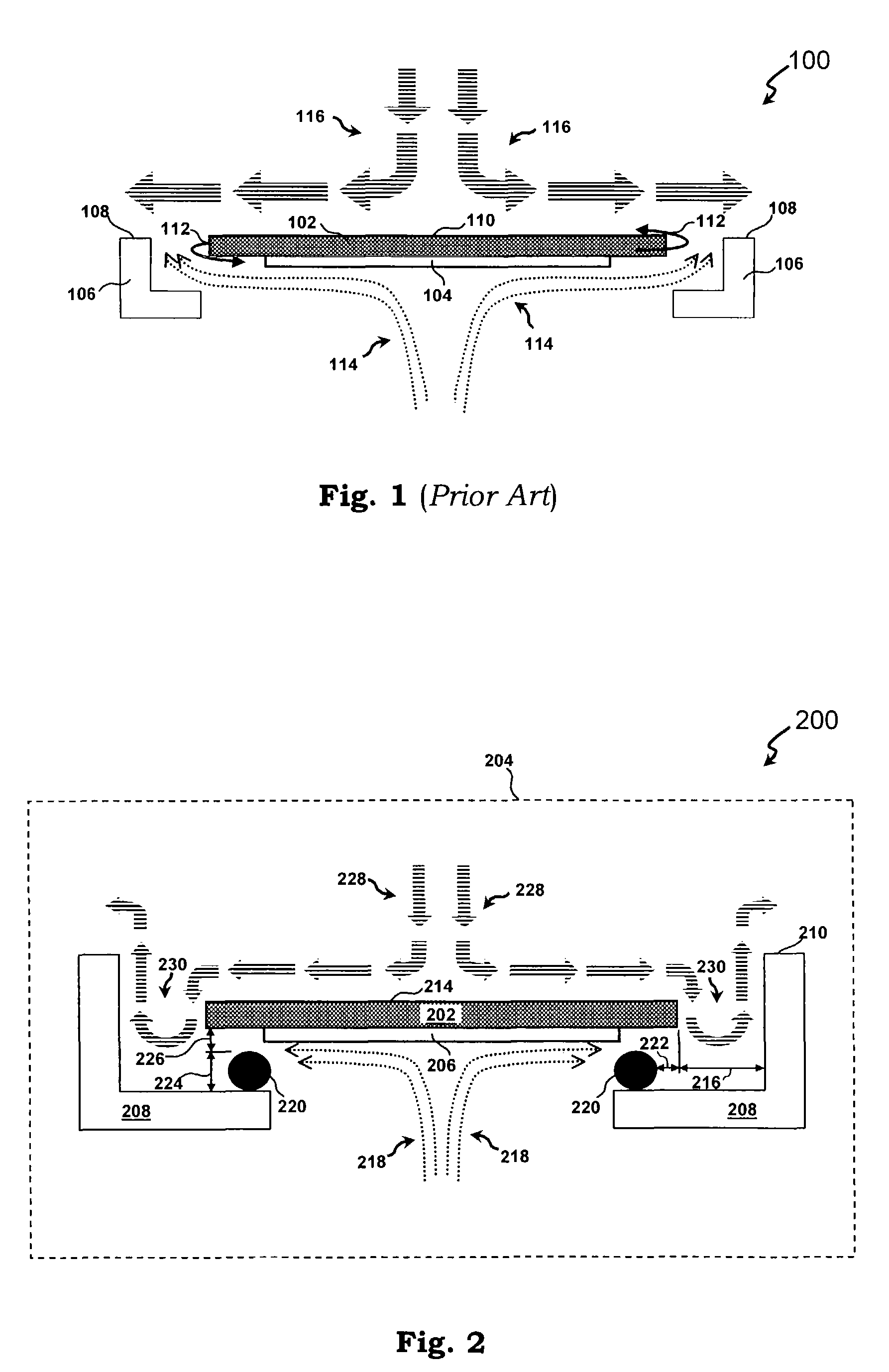
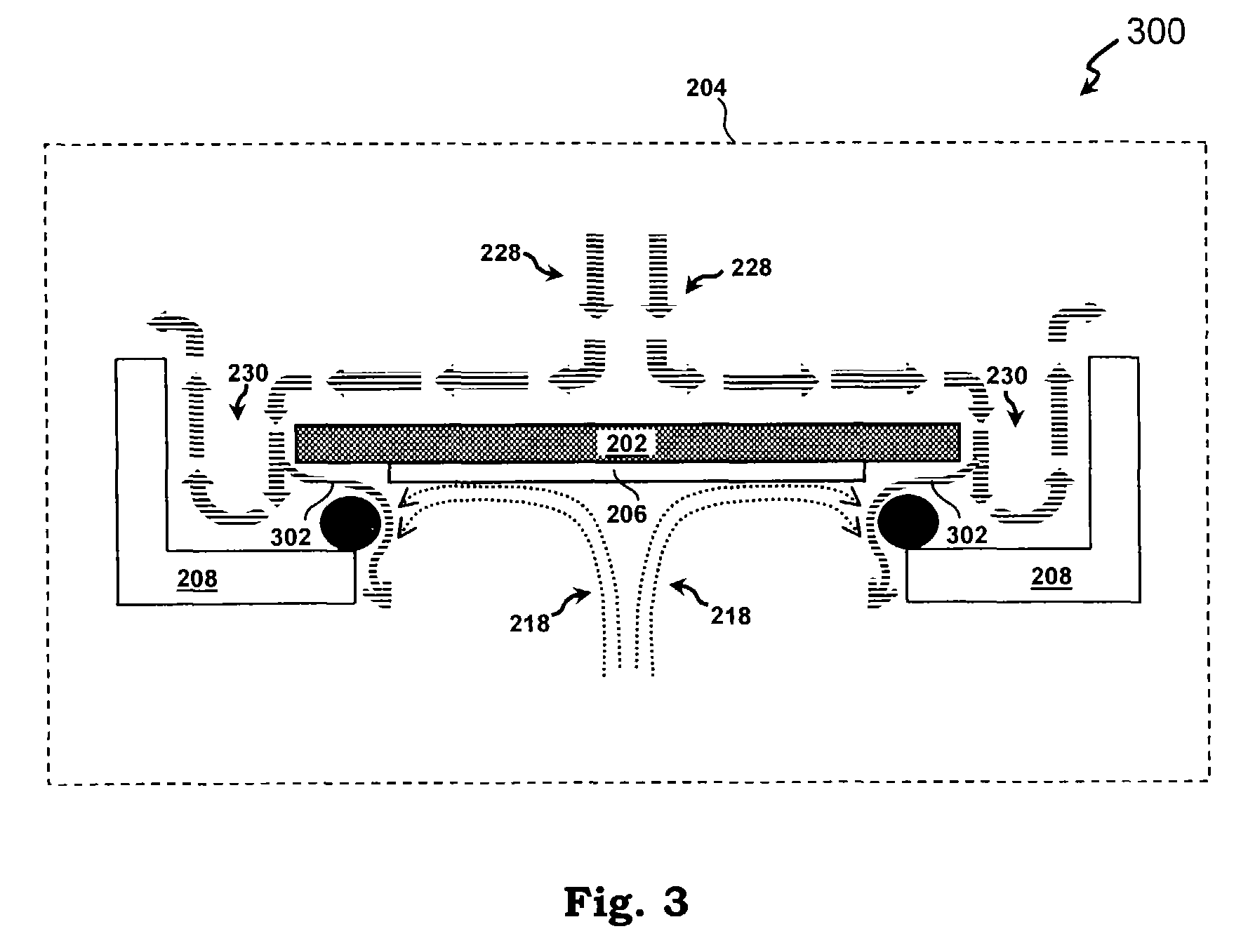
[0018]The present invention provides a versatile system for remediating aberrations along the outer perimeter of a semiconductor wafer, particularly along the edge. Specifically, the present invention defines a system that safely remediates peeling, blistering and other structural anomalies occurring along a wafer's edge without significantly affecting active area on the wafer. The present invention recognizes that edge aberrations often occur in the u...


PUM


Abstract

The present invention provides a system (200, 300) for remediating aberrations along the perimeter of a semiconductor wafer (202). The system includes a cleaning apparatus (204) within which the wafer is spun within a confined area. A chuck (208) defines the confined area, having a sidewall that extends above the upper surface (214) of the wafer and surrounds the perimeter of the wafer. The chuck also has a bottom wall, with an aperture formed therein, beneath the wafer. The system includes an isolation barrier (220), disposed atop the bottom wall of the chuck and around the aperture, in proximity to the lower surface so of the wafer. This forms a narrow gap (226) between the barrier and the wafer. A pressurized source forcefully directs a gas (218) at and along the lower surface of the wafer. The system also includes a remediation solution (228) that is applied to the upper surface of the wafer. The solution is forced into a well (230) formed between the chuck sidewall and the perimeter of the wafer, such that the solution bathes the perimeter of the wafer.

Description

TECHNICAL FIELD OF THE INVENTION[0001]The present invention relates generally to the field of semiconductor devices and, more particularly, to apparatus and methods for remediating aberrations around the outer edge or perimeter of a substrate during device fabrication.BACKGROUND OF THE INVENTION[0002]The continual demand for enhanced integrated circuit performance has resulted in, among other things, a dramatic reduction of semiconductor device geometries, and continual efforts to optimize the production and performance of every substructure within any semiconductor device. A number of improvements and innovations in fabrication processes, material composition, and layout of the active circuit levels of a semiconductor device have resulted in very high-density circuit designs. Increasingly dense circuit design has not only improved a number of performance characteristics, it has also increased the importance of—and attention to—maximum utilization and yield of wafer real estate.[000...

Claims


Application Information

Patent Timeline
Patent Type & Authority Patents(United States)
IPC IPC(8): B08B3/02B08B3/10B08B5/02H01L21/00
CPCB08B3/02B08B3/102H01L21/67051B08B5/02Y10S134/902
Inventor XIA, CHANGFENGHURD, TRACE Q.
Owner TEXAS INSTR INC
Why Eureka
Try Eureka