Dielectric waveguide filter with inductive windows and coplanar line coupling

a filter and dielectric waveguide technology, applied in waveguides, instruments, resonators, etc., can solve the problems of difficult connection of the filter to a planar circuit and the drawback of the filter type in larger dimensions, and achieve excellent filter characteristics

Inactive Publication Date: 2007-03-27
NEC CORP
View PDF14 Cites 12 Cited by
  • Summary
  • Abstract
  • Description
  • Claims
  • Application Information

AI Technical Summary

Benefits of technology

[0008]In view of the above, it is an object of the present invention to provide a small-dimension filter having a dielectric waveguide tube structure and excellent filter characteristics even in the case of a smaller number of stages, and to provide a filter capable of being mounted by a flip-chip mounting technique without providing a particular external terminal thereto for connection with a planar circuit.

Problems solved by technology

This type of the filters has a drawback in larger dimensions although it is superior in the performance thereof.
In addition, it is generally difficult to connect the filter to a planar circuit.
This results from the fact that the electromagnetic field in the micro-strip line is distributed up to the top portion thereof and can thus be susceptible to the effects of attaching a cap member thereto.

Method used


Image

  • Dielectric waveguide filter with inductive windows and coplanar line coupling
  • Dielectric waveguide filter with inductive windows and coplanar line coupling
  • Dielectric waveguide filter with inductive windows and coplanar line coupling

Examples


first embodiment

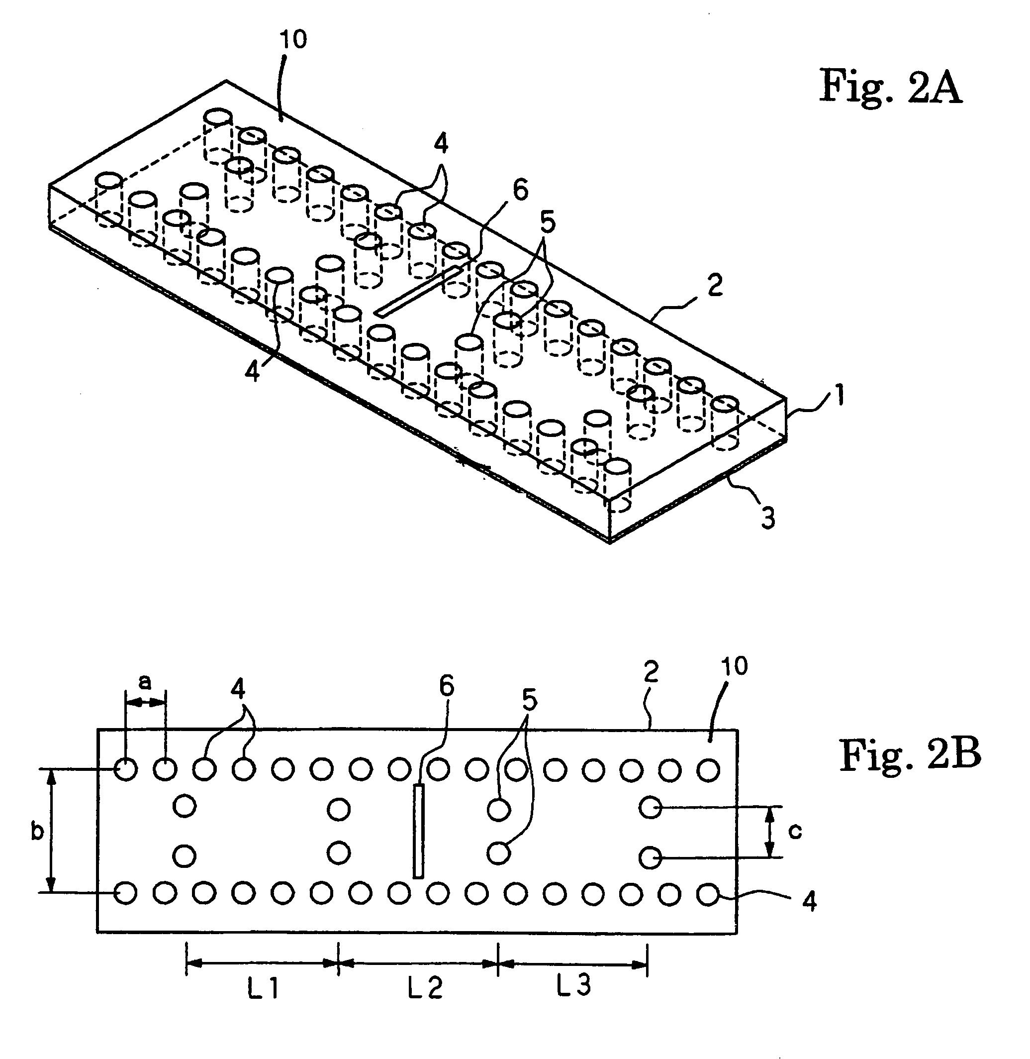
[0033]Hereinafter, the present invention is more specifically described based on the preferred embodiments thereof with reference to the drawings. Like reference labels in different drawing figures refer to the same feature and may be described in detail for all drawing figures. Referring to FIGS. 2A and 2B, there is shown the schematic structure of a filter 10 according to the present invention. FIGS. 2A and 2B show the schematic structure of a filter 10 having a three-stage configuration. FIG. 2A is a perspective view thereof, whereas FIG. 2B is a top plan view thereof. A dielectric substrate 1 is provided with a pair of longer-side conductor planes, relative to the rectangular waveguide filter cross-section, a top conductor 2 formed on a surface thereof, and a bottom conductor 3 formed on the opposing surface thereof. Via-holes 4 connecting together the top conductor 2 and the bottom conductor 3 are formed in two rows parallel to a signal transfer direction. The spacing “a” (FIG....

second embodiment

[0039]Referring to FIGS. 4A and 4B, there is shown the schematic structure of a filter 10 according to the present invention. FIGS. 4A and 4B show the schematic structure of a filter 10 having a four-stage configuration. FIG. 4A is a perspective view thereof, whereas FIG. 4B is a top plan view thereof. A dielectric substrate 1 is provided with a top conductor 2 formed on one surface thereof, and a bottom conductor 3 formed on the opposite surface thereof. Via-holes 4 connecting the top conductor 2 and the bottom conductor 3 (FIG. 4A) together are formed in two rows along the signal transfer direction. Side conductor planes 20 and 30 are not shown, but are present as in FIG. 2A. It is preferable that the spacing “a” (FIG. 4B) between adjacent via-holes be equal to or less than ½ of the in-tube wavelength. This structure can be construed as a pseudo waveguide tube having a waveguide-tube cross section defined by the thickness of the dielectric and the spacing “b” (FIG. 4B) between the...

fourth embodiment

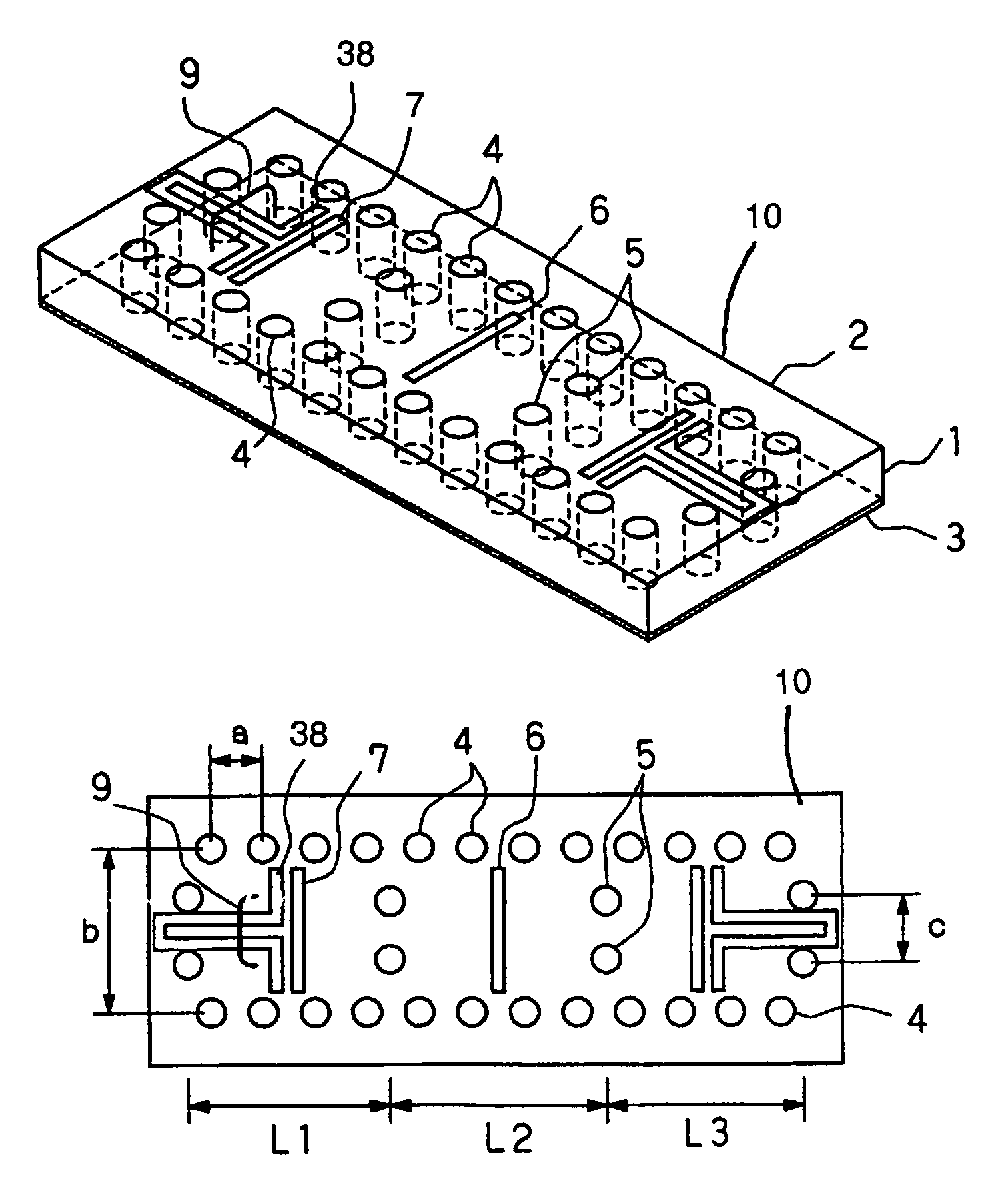
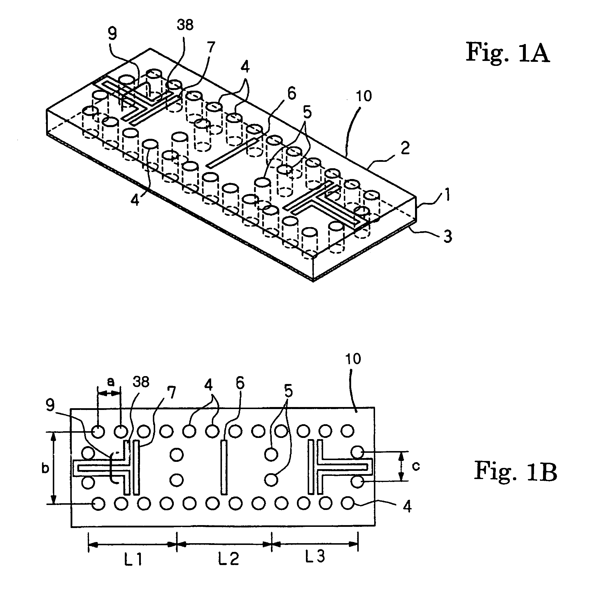
[0043]Referring to FIGS. 1A and 1B, there is shown the schematic structure of a filter 10 according to the present invention. FIGS. 1A and 1B show the schematic structure of a filter 10 having a three-stage configuration. FIG. 1A is a perspective view thereof, whereas FIG. 1B is a top plan view thereof. This embodiment best exhibits the features of the present invention. A dielectric substrate 1 (FIG. 1A) is provided with a top conductor 2 formed on one surface thereof, and a bottom conductor 3 formed on the opposite surface thereof. Via-holes 4 connecting together the top conductor 2 and the bottom conductor 3 are formed in two rows along the signal transfer direction. The spacing “a” (FIG. 1B) between adjacent via-holes is preferably equal to or smaller than ½ of the in-tube wavelength. This structure is construed as a pseudo waveguide tube having a waveguide-tube cross section defined by the thickness of the dielectric and the spacing “b” (FIG. 1B) between the via-holes 4 arrange...


PUM


Abstract

The present invention provides a filter exhibiting excellent filter characteristics and having less number of stages. A dielectric substrate (1) has one surface connected to a top conductor (2) and an opposite surface connected to a bottom conductor (3). A pair of rows of via-holes connecting together the top conductor (2) and the bottom conductor (3) are formed along the signal transfer direction. A slit (6) is formed in a portion of the top conductor (2) overlying the central resonator among a plurality of resonators. The slit (6) extends in a direction perpendicular to the signal transfer direction. Slits (7, 8) are formed in each of portions of the top conductor (2) overlying resonators disposed at both ends. A coplanar waveguide (9) mounted on the top conductor (2) is connected to the slit (7).

Description

TECHNICAL FIELD[0001]The present invention relates to a filter having a waveguide tube structure for use as a high-frequency component.TECHNICAL BACKGROUND[0002]Typical waveguide tube filters used in microwave and millimeter-wave bands are realized by using a resonator structure including a metallic waveguide tube formed in a drawn structure. This type of the filters has a drawback in larger dimensions although it is superior in the performance thereof.[0003]Thus, as recited in JP Patent Application 10-82184, a pseudo waveguide tube band-pass filter is devised which has a side wall of the waveguide tube configured by metallic via-holes in a dielectric substrate. As a practical example, FIGS. 9A and 9B show the schematic structure of a filter 10 having a four-stage configuration. FIG. 9A is a perspective view thereof, whereas FIG. 9B is a top plan view thereof. Referring to FIG. 9A, a top conductor 2 is formed on one of the surfaces of the dielectric substrate 1, whereas a bottom con...

Claims


Application Information

Patent Timeline
Patent Type & Authority Patents(United States)
IPC IPC(8): H01P1/20H01P1/205H01P1/208H01P5/08H01P5/107
CPCH01P1/2088
Inventor MARUHASHI, KENICHIITO, MASAHARUOHATA, KEIICHI
Owner NEC CORP
Why Eureka
Try Eureka