Methods of forming pluralities of capacitors

a technology of capacitors and capacitor electrodes, which is applied in the direction of capacitors, semiconductor devices, electrical equipment, etc., can solve the problems of capacitor electrode toppling, difficulty in etching the capacitor electrode openings within the insulative material,

Active Publication Date: 2007-04-03
MICRON TECH INC
View PDF57 Cites 127 Cited by
  • Summary
  • Abstract
  • Description
  • Claims
  • Application Information

AI Technical Summary

Problems solved by technology

As integrated circuitry density has increased, there is a continuing challenge to maintain sufficiently high storage capacitance despite typical decreasing capacitor area.
However, it can be difficult to etch the capacitor electrode openings within the insulative material, particularly where the openings are deep.
This can lead to toppling of the capacitor electrodes either during the etch to expose the outer sidewall surfaces, during transport of the substrate, and / or during deposition of the capacitor dielectric layer or outer capacitor electrode layer.

Method used


Image

  • Methods of forming pluralities of capacitors
  • Methods of forming pluralities of capacitors
  • Methods of forming pluralities of capacitors

Examples


Embodiment Construction

[0035]This disclosure of the invention is submitted in furtherance of the constitutional purposes of the U.S. Patent Laws “to promote the progress of science and useful arts” (Article 1, Section 8).

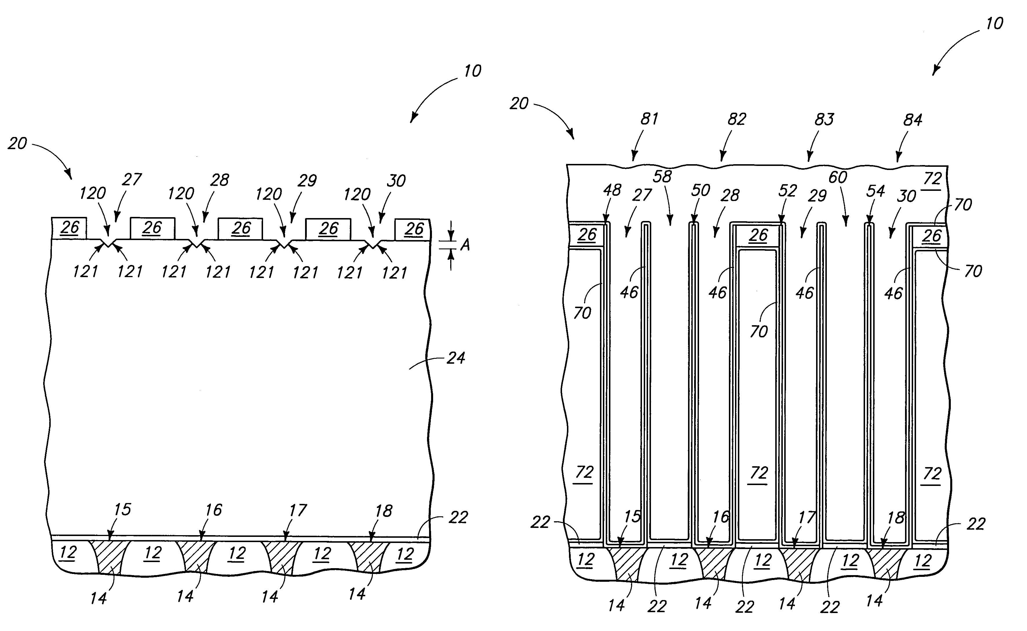
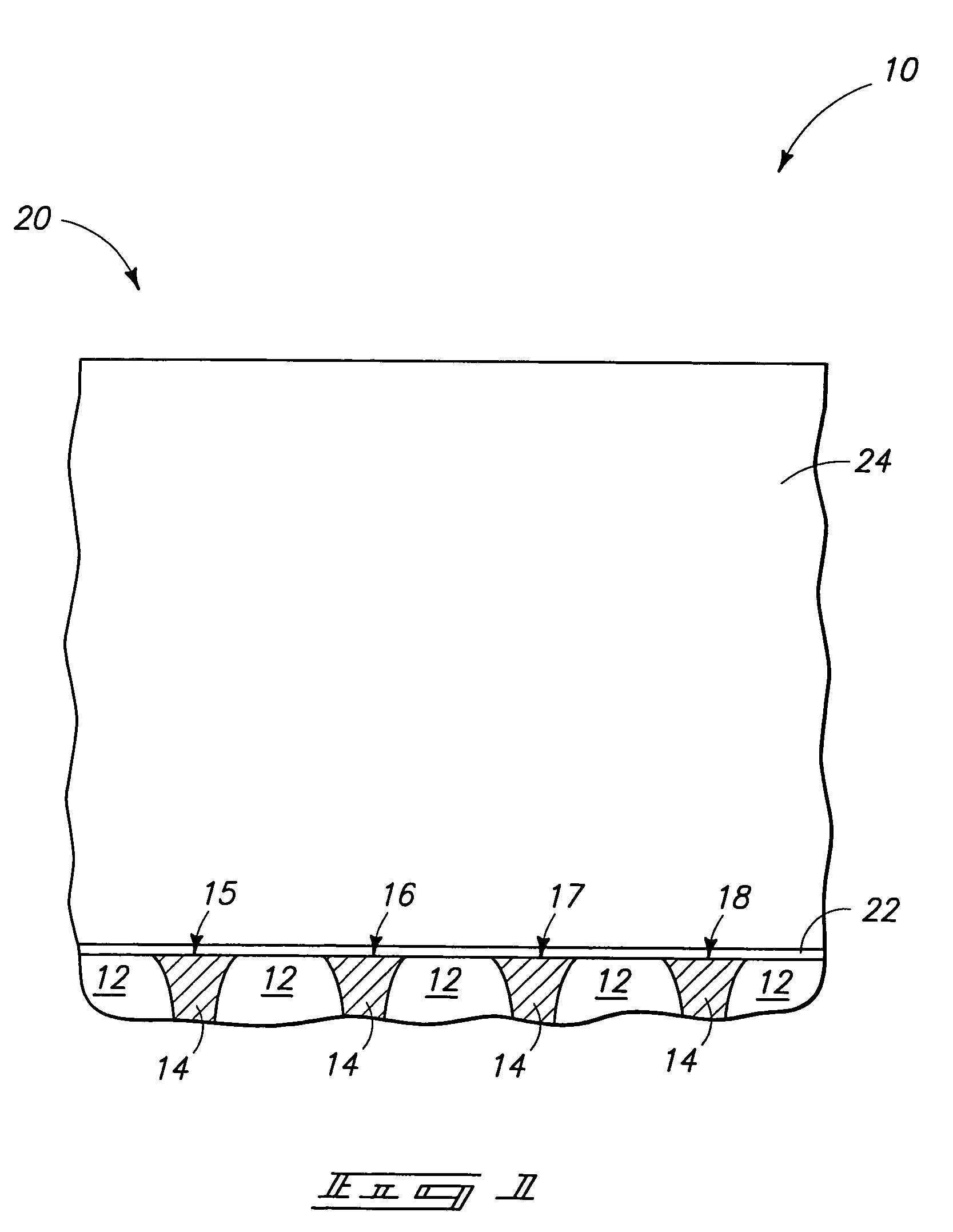
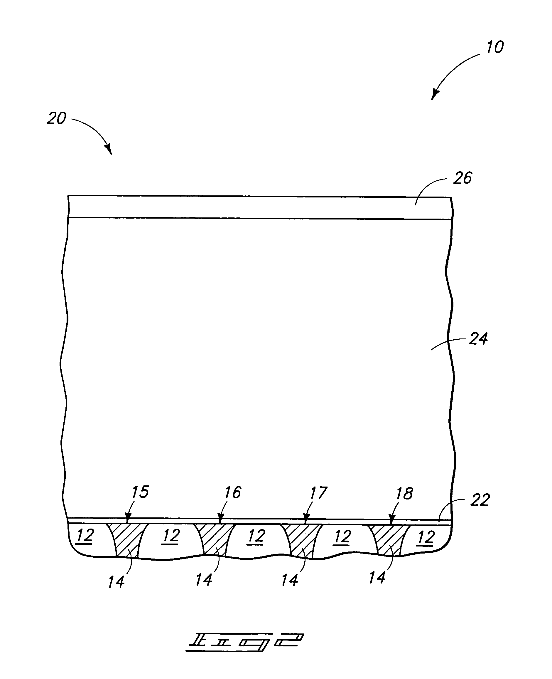
[0036]Exemplary preferred methods of forming a plurality of capacitors are described with reference to FIGS. 1–26. FIG. 1 depicts a substrate 10 preferably comprising a semiconductor substrate. In the context of this document, the term “semiconductor substrate” or “semiconductive substrate” is defined to mean any construction comprising semiconductive material, including, but not limited to, bulk semiconductive materials such as a semiconductive wafer (either alone or in assemblies comprising other materials thereon), and semiconductive material layers (either alone or in assemblies comprising other materials). The term “substrate” refers to any supporting structure, including, but not limited to, the semiconductive substrates described above. Accordingly and by way of example only, FIG. ...


PUM

PropertyMeasurementUnit
depthaaaaaaaaaa
depthaaaaaaaaaa
thicknessaaaaaaaaaa

Abstract

The invention comprises methods of forming pluralities of capacitors. In one implementation, metal is formed over individual capacitor storage node locations on a substrate. A patterned masking layer is formed over the metal. The patterned masking layer comprises openings therethrough to an outer surface of the metal. Individual of the openings are received over individual of the capacitor storage node locations. A pit is formed in the metal outer surface within individual of the openings. After forming the pits, the metal is anodically oxidized through the openings effective to form a single metal oxide-lined channel in individual of the openings over the individual capacitor storage nodes. Individual capacitor electrodes are formed within the channels in electrical connection with the individual capacitor storage node locations. At least some of the metal oxide is removed from the substrate, and the individual capacitor electrodes are incorporated into a plurality of capacitors. Other aspects and implementations are contemplated.

Description

TECHNICAL FIELD[0001]This invention relates to methods of forming pluralities of capacitors.BACKGROUND OF THE INVENTION[0002]Capacitors are one type of component which is commonly used in the fabrication of integrated circuits, for example in DRAM circuitry. A typical capacitor is comprised of two conductive electrodes separated by a non-conducting dielectric region. As integrated circuitry density has increased, there is a continuing challenge to maintain sufficiently high storage capacitance despite typical decreasing capacitor area. The increase in density of integrated circuitry has typically resulted in greater reduction in the horizontal dimension of capacitors as compared the vertical dimension. In many instances, the vertical dimension of capacitors has increased.[0003]One manner of forming capacitors is to initially form an insulative material within which a capacitor storage node electrode is formed. For example, an array of capacitor electrode openings for individual capa...

Claims


Application Information

Patent Timeline
Patent Type & Authority Patents(United States)
IPC IPC(8): H01L21/8242H01L21/20
CPCH01L27/10852H01L28/91H01L27/10817H10B12/318H10B12/033
Inventor SANDHU, GURTEJ S.MANNING, H. MONTGOMERYKRAMER, STEPHEN J.
Owner MICRON TECH INC
Why Eureka
Try Eureka