
Delay-locked loop device capable of anti-false-locking and related methods
a loop device and delay-locked technology, applied in the direction of electrical equipment, pulse automatic control, etc., can solve problems such as delay, and achieve the effect of simplifying the delay-locked loop devi
- Summary
- Abstract
- Description
- Claims
- Application Information
AI Technical Summary
Benefits of technology
Problems solved by technology
Method used
Image

Examples
Embodiment Construction
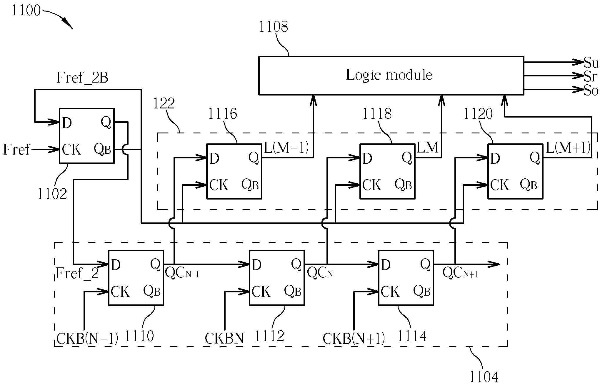
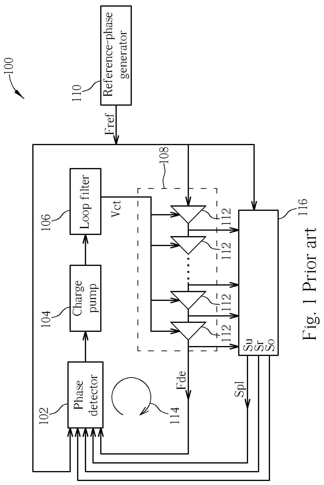
[0025]Please refer to FIG. 6, which illustrates a flowchart of a process 600 for simplifying a DLL device in accordance with the present invention. The process 600 is utilized for simplifying DLL devices such as the DLL device 100 shown in FIG. 1, and includes the following steps:
[0026]Step 602: start.
[0027]Step 604: reverse phases outputted from delay units of a voltage control delay circuit.
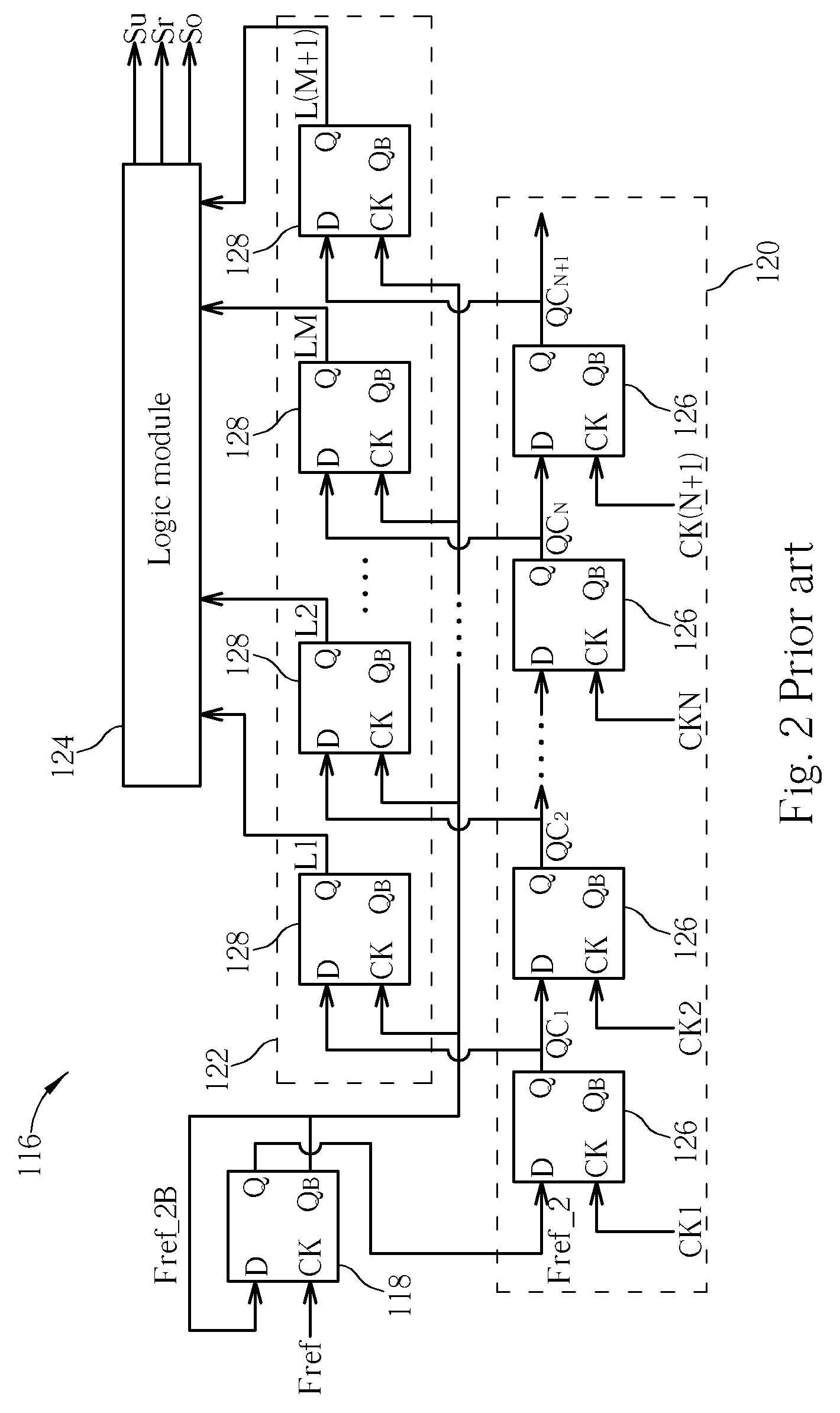
[0028]Step 606: transmit the reversed phases in step 604 to shift registers in a first shift register set corresponding to the delay units of the voltage control delay circuit, so as to generate a first sequence of comparison signals according to a first divided phase and inverse phases of phases outputted from the delay units of the voltage control delay circuit;
[0029]Step 608: remove a plurality of shift registers in the first shift register set corresponding to a plurality of delay units of initial stages of the voltage control delay circuit according to a default requirement;
[0030]Step 610:...
PUM
 Abstract
Description
Claims
Application Information