Circuit configurations having four terminal JFET devices

a technology of junction field effect transistor and circuit configuration, which is applied in the direction of logic circuits, logic circuits characterised by logic functions, pulse techniques, etc., can solve the problems of loss of integrity in operation or over time, difficulty or high cost of manufacturing of thin gate insulating layers, and approaching scaling limits of cmos technology

Inactive Publication Date: 2007-11-15
MIE FUJITSU SEMICON
View PDF39 Cites 73 Cited by
  • Summary
  • Abstract
  • Description
  • Claims
  • Application Information

AI Technical Summary

Problems solved by technology

However, as device feature sizes decrease, CMOS technology is approaching scaling limits.
Such thin gate insulating layers can become difficult or expensive to manufacture and / or lose integrity in operation or over time.

Method used


Image

  • Circuit configurations having four terminal JFET devices
  • Circuit configurations having four terminal JFET devices
  • Circuit configurations having four terminal JFET devices

Examples


Embodiment Construction

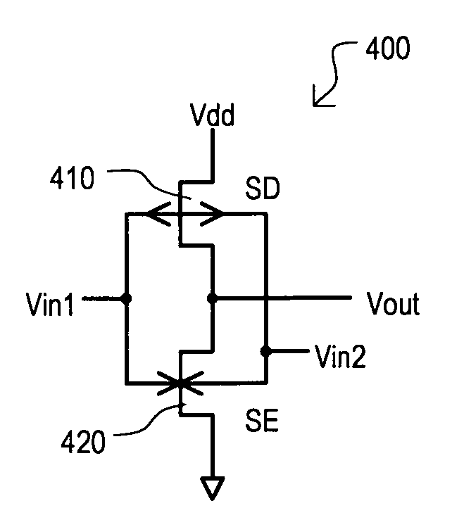
[0041]Various embodiments of the present invention will now be described in detail with reference to a number of drawings. The embodiments show circuits formed with four-terminal (4T) junction field effect transistors (JFET), including complementary 4T JFETs.

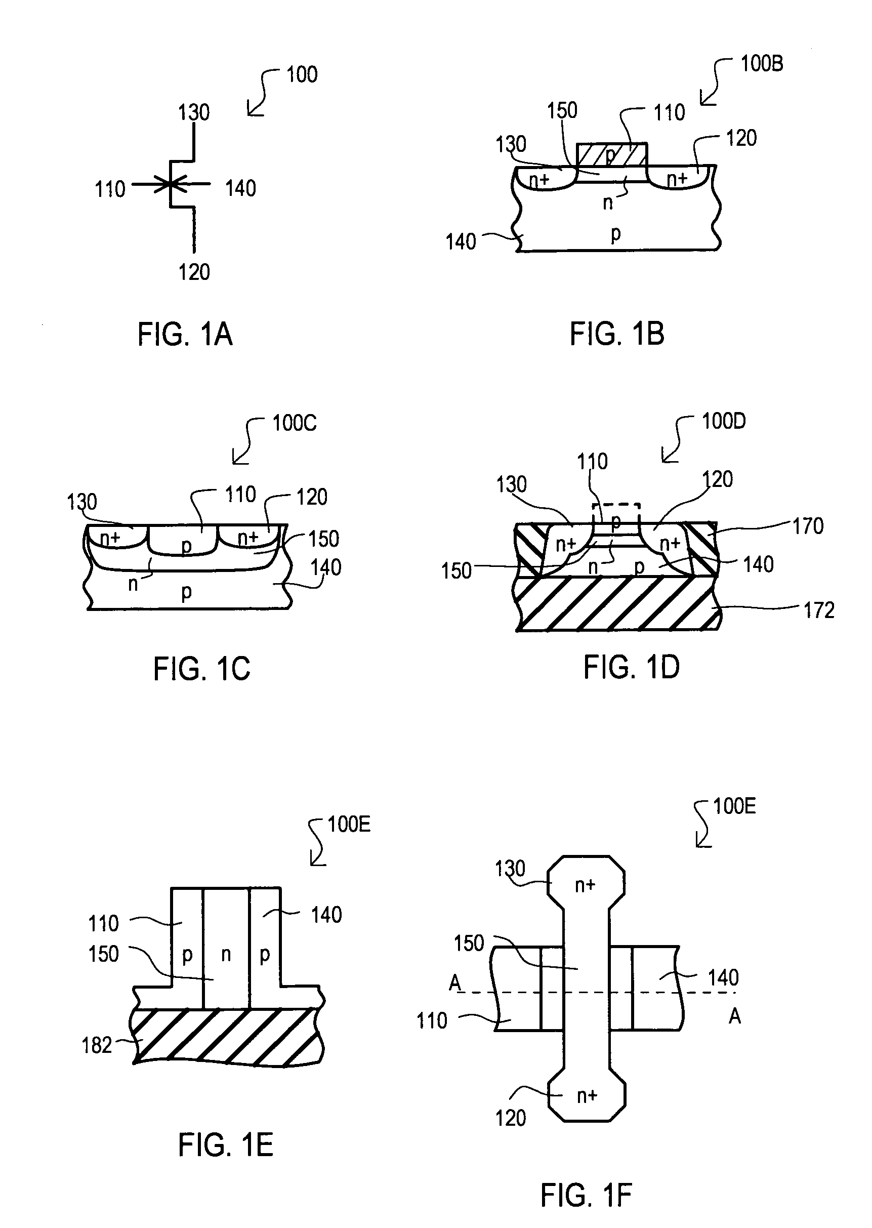
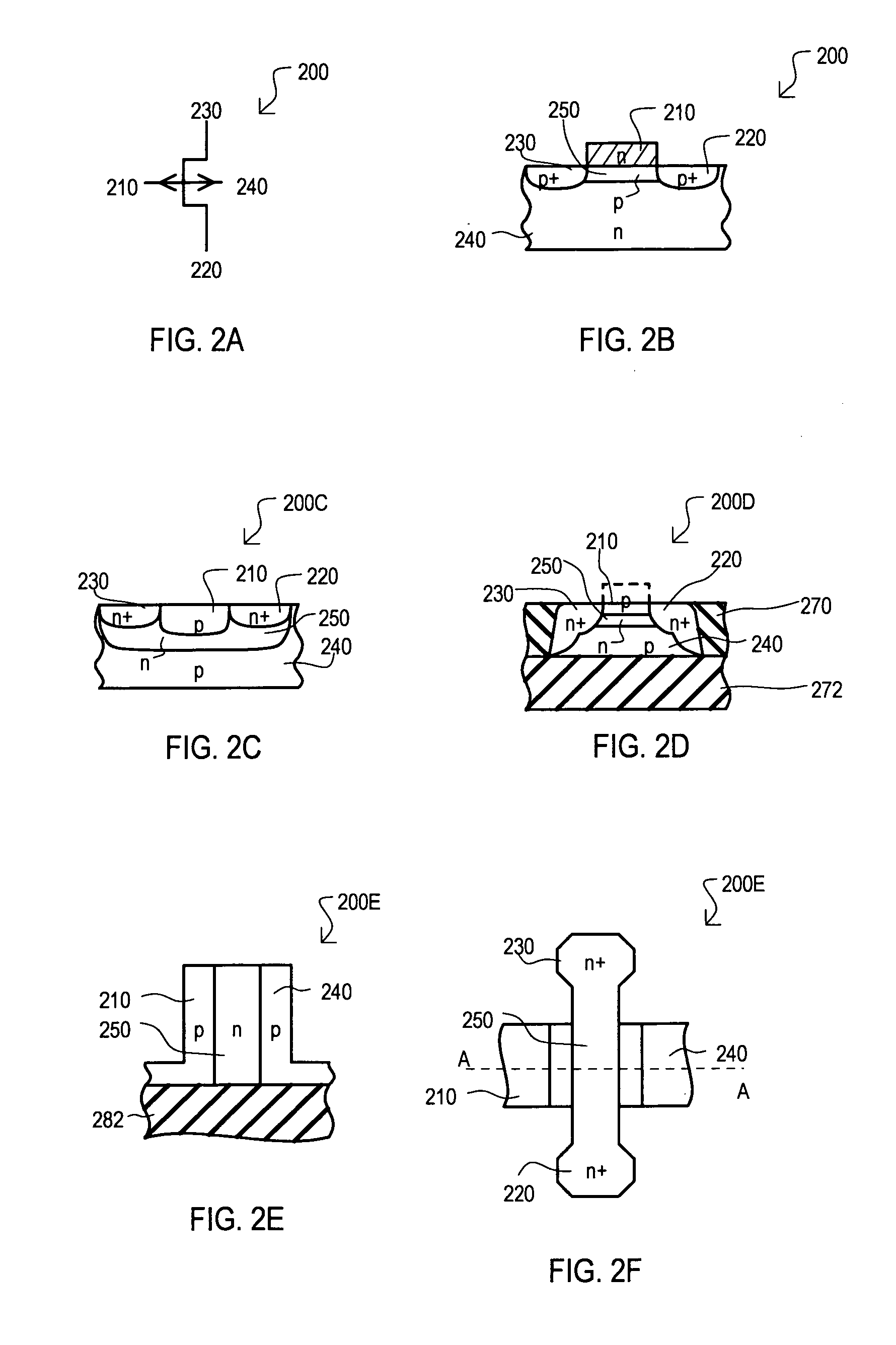
[0042]The disclosed embodiments can include circuits formed with 4T JFETs of either n-channel or p-channel conductivity types. Such devices provide separate control of a channel between a source and drain by application of both a gate potential and a “back” gate potential. Two of the many possible configurations for such devices are shown in FIGS. 1A to 2B.

[0043]FIG. 1A is a schematic representation of a 4T n-channel JFET according to an embodiment, hereinafter referred to as a 4T NFET, and designated by the general reference character 100. A 4T NFET 100 can include a front gate 110, a source 120, a drain 130, a back gate (in this example a well) 140 and channel region 150. Both front gate 110 and back gate 140 can be used to co...


PUM


Abstract

Circuits using four terminal junction field effect transistors (JFETs) are disclosed. Such circuits can include various static and dynamic logic circuits, flip-flops, multiplexer, tri-state driver, phase detector, logic having variable speeds of operation, and/or analog circuit with such four terminal JFETs operating in a linear or nonlinear mode.

Description

[0001]This application claims the benefit of U.S. Provisional Patent Application Ser. No. 60 / 799,787, filed May 11, 2006, the contents of which are incorporated by reference herein.TECHNICAL FIELD[0002]The present invention relates generally to semiconductor circuits, and more particularly to semiconductor circuits using junction field effect transistor (JFET) devices.BACKGROUND OF THE INVENTION[0003]Conventional junction field effect transistors (JFETs) are known. FIG. 19 shows a schematic diagram of a conventional n-channel JFET 1900. Conventional n-channel JFET operates as a three terminal device, including a control gate 1910, drain 1920, and source 1930. In operation, conventional JFET 1900 functions as a depletion mode device, providing a relatively low impedance path between source 1930 and drain 1920. In response to a voltage applied at control gate 1910, a depletion region can be altered to change the conductivity between source 1930 and drain 1920.[0004]Currently, for most...

Claims


Application Information

Patent Timeline
Patent Type & Authority Applications(United States)
IPC IPC(8): H03K19/00H01L25/00
CPCH01L29/785H01L29/8086H03K19/09403H01L2029/7857H01L2924/0002H01L2924/00H01L29/66893
Inventor KAPOOR, ASHOK KUMAR
Owner MIE FUJITSU SEMICON
Why Eureka
Try Eureka