Low temperature production of large-grain polycrystalline semiconductors

a polycrystalline semiconductor and low temperature technology, applied in the field of low temperature production of large-grain polycrystalline semiconductors, can solve the problems of requiring high annealing temperature and annealing time in tens of hours, and high annealing temperature can be destructive to various device constructions

Inactive Publication Date: 2007-04-10
THE BOARD OF TRUSTEES OF THE UNIV OF ARKANSAS
View PDF14 Cites 47 Cited by
  • Summary
  • Abstract
  • Description
  • Claims
  • Application Information

AI Technical Summary

Benefits of technology

[0014]It has now been found that formation of a thin oxide layer on an amorphous semiconductor, followed by application of a metal layer and annealing, leads to formation of large-grain crystallites in the previous amorphous layer. Hence, an amorphous region of a semiconductor can be converted to an at least partially crystalline region by: (i) at least partially oxidizing the amorphous region of the semiconductor; (ii) applying a contact metal to a surface of the at least partially oxidized amorphous region; and (iii) annealing t

Problems solved by technology

It is still the preferred method to obtain poly-Si films, however its main disadvantage is that it requires high annealing temperatures and annealing times in tens of hours.
The

Method used


Image

  • Low temperature production of large-grain polycrystalline semiconductors
  • Low temperature production of large-grain polycrystalline semiconductors
  • Low temperature production of large-grain polycrystalline semiconductors

Examples


examples

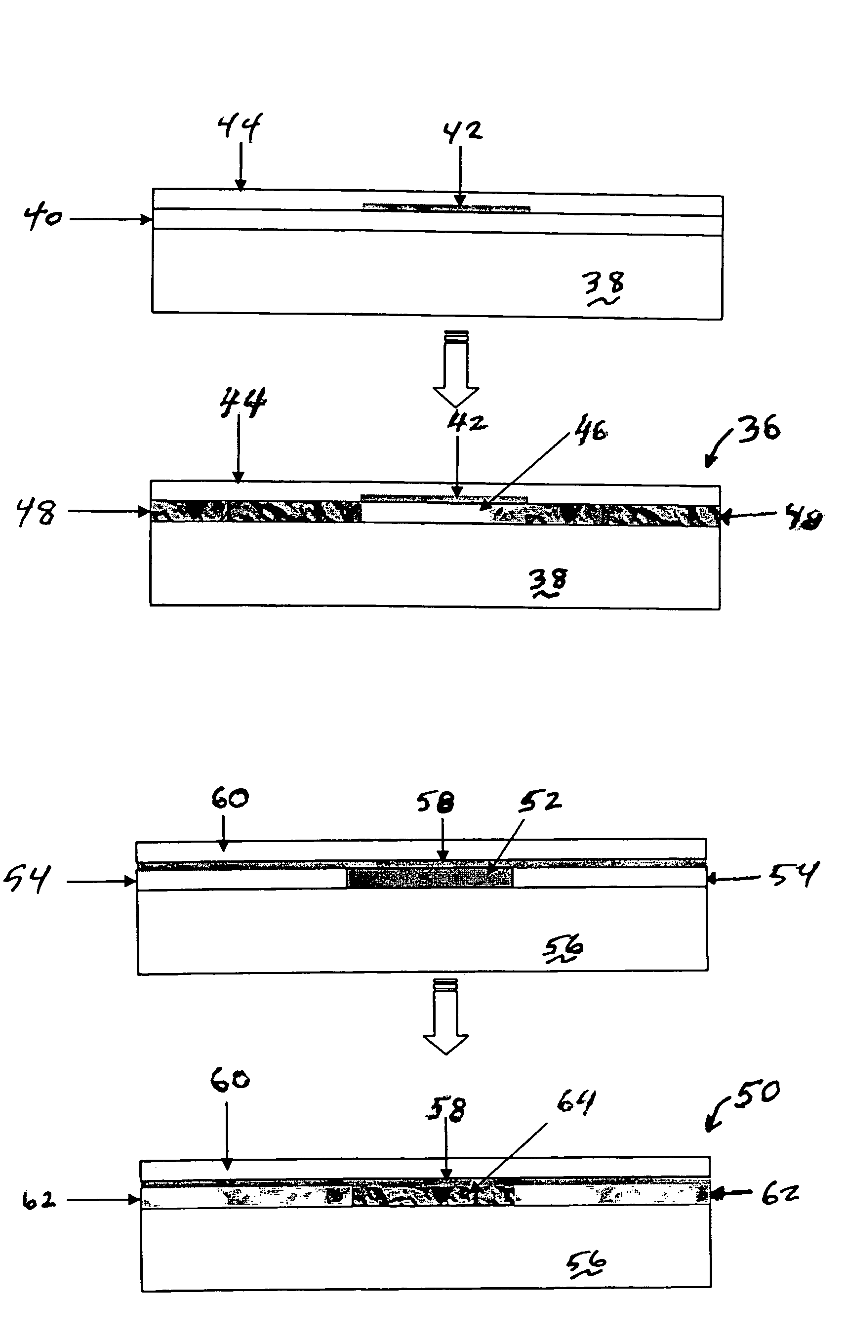
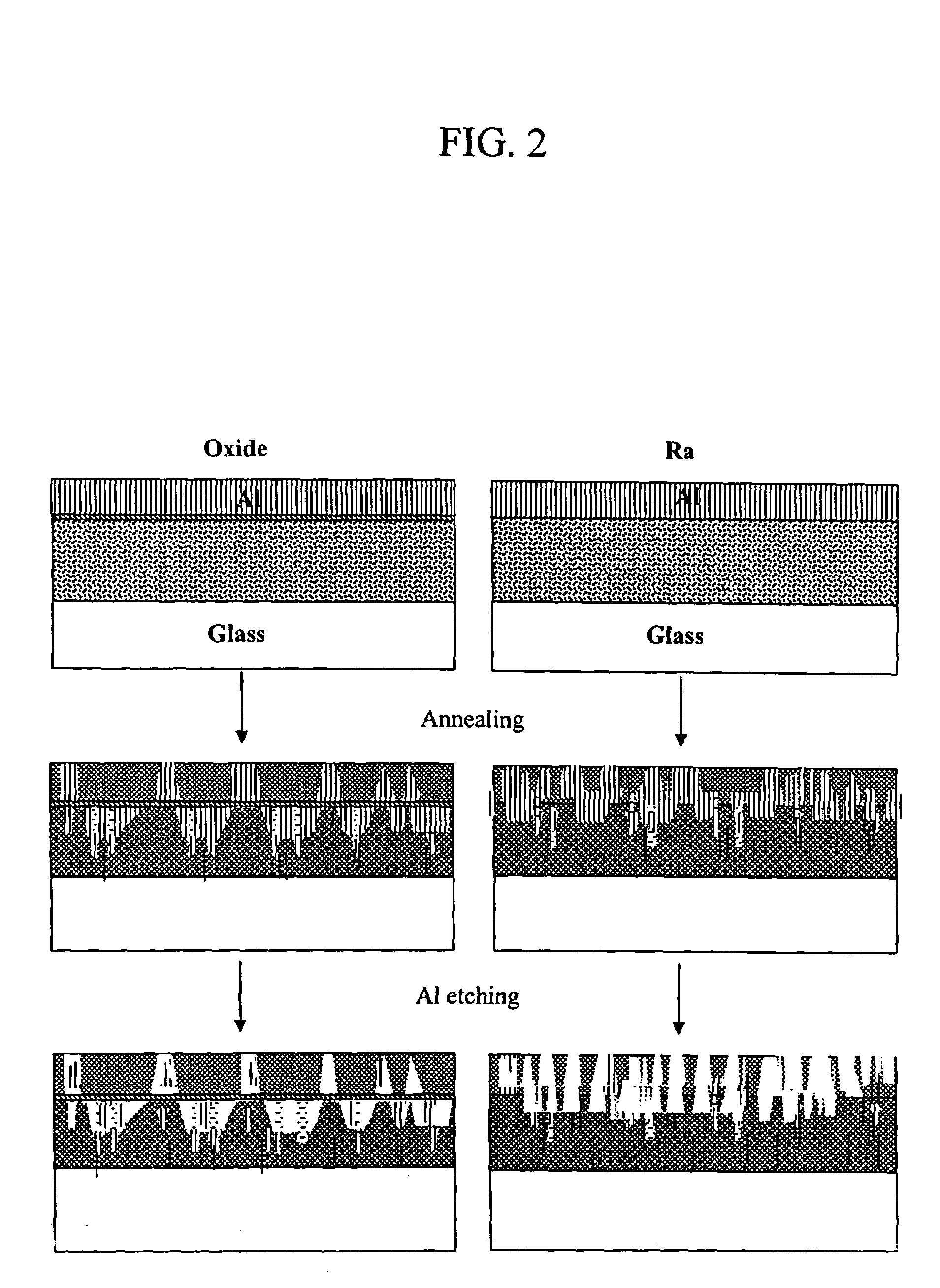
[0052]In order to investigate the effect of a native SiO2 layer on MIC, two experiments were carried out. In the first experiment, three samples were prepared on Corning 7059 glass substrates in a multi-chamber plasma-enhanced chemical vapor deposition (PECVD) system. The samples consisted of 3000 Å thick undoped a-Si:H deposited on the glass substrate, which were then capped with 2000 Å thick sputtered Al. The base pressure prior to all depositions was in the range of 6×10⁻⁸ torr. For the first sample, the Al was deposited right after (RA) the completion of the a-Si:H deposition. The sample remained under vacuum during preparation so it was not exposed to the atmosphere. For the second sample (10 M), the a-Si:H layer was exposed to room ambient for 10 minutes to allow for some native oxide layer to form prior to aluminum deposition. For the third sample (2 D), the a-Si:H layer was exposed to room ambient for 2 days to form an even thicker native oxide layer. The oxide layer thickne...


PUM


Abstract

An oxide or nitride layer is provided on an amorphous semiconductor layer prior to performing metal-induced crystallization of the semiconductor layer. The oxide or nitride layer facilitates conversion of the amorphous material into large grain polycrystalline material. Hence, a native silicon dioxide layer provided on hydrogenated amorphous silicon (a-Si:H), followed by deposited Al permits induced crystallization at temperatures far below the solid phase crystallization temperature of a-Si. Solar cells and thin film transistors can be prepared using this method.

Description

CROSS-REFERENCE TO RELATED APPLICATION[0001]The present application claims the benefit of priority of U.S. Provisional Application 60 / 513,670, filed Oct. 23, 2003, the disclosure of which is incorporated herein by reference.STATEMENT OF GOVERNMENT SUPPORT[0002]Development of this invention was supported at least in part by the U.S. Department of Energy through DOE / EPSCOR grant 0402-03027-21-0000. The Government may have certain rights in the invention.BACKGROUND OF THE INVENTION[0003]Silicon (Si) has been and still is the center of attention for much work in the world of semiconductors and is still the material of choice for most semiconductor applications. Among the reasons for this are the relative ease of growing c-Si and poly-Si compared to other materials, the relative low number of defects that usually accompany this growth, and finally, the ease of growing SiO2 on Si, which furnishes a dielectric / Si interface with very unique characteristics that make Si far more superior tha...

Claims


Application Information

Patent Timeline
IPC IPC(8): H01L21/20H01L29/76
CPCH01L21/02422H01L21/02521H01L21/02532H01L21/02672H01L29/66757H01L29/78675H01L31/1872Y02E10/50Y02P70/50
Inventor NASEEM, HAMEED A.ALBARGHOUTI, MARWAN
Owner THE BOARD OF TRUSTEES OF THE UNIV OF ARKANSAS
Why Eureka
Try Eureka