Thin film transistor, display device and their production

a thin film transistor and display device technology, applied in transistors, thermoelectric devices, nano-informatics, etc., can solve the problems of increasing light leakage current, low pattern accuracy of electrodes, and adverse effects, and achieve the effect of improving the orientation order of organic semiconductor molecules

Inactive Publication Date: 2007-04-10
HITACHI LTD
View PDF2 Cites 3 Cited by
  • Summary
  • Abstract
  • Description
  • Claims
  • Application Information

AI Technical Summary

Benefits of technology

[0009]As described above, conventional coating with a SAM on the surface of the insulation film to be a substrate has a problem of the increase in the light leakage current, while improving the order of orientations of organic semiconductor molecules in an organic semiconductor film, and a switching performance such as electric field-effect mobility and an on / off ratio of the current. This is because the coating of a SAM has improved the orientation order of the organic semiconductor molecules in the organic semiconductor film not only formed in a gate electrode-projected region on the surface of the insulation film, which controls a switching performance such as an electric field-effect mobility and an on / off ratio of the current, but also formed outside the gate electrode-projected region which controls a light leakage current.
[0011]As described above, in an organic thin film transistor, the modification of the surface of the insulation film with a self assembled monolayer film, for improving the orientation order of the organic semiconductor molecules and improving the switching performance, has a problem of increasing the light leakage current and being incapable of finely forming the electrode with a coating process.
[0012]To solve the above problem, according to the invention, a thin film transistor is provided having a gate electrode, a gate insulation film, a source electrode, a drain electrode, a semiconductor film and a protection film, stacked on a substrate, in which the semiconductor film is composed of an aggregate of organic semiconductor molecules, and the orientation order of the organic semiconductor molecules of the semiconductor film formed in a gate electrode-projected region on the surface of the insulation film is higher than that of the semiconductor film formed outside the region. In particular, a method for forming the organic semiconductor film having the above characteristics is provided which comprises selectively disposing a self assembled monolayer film on the surface of the insulation film and then forming an organic semiconductor film thereon by making use of the property that the orientation order of the organic semiconductor film formed on the self assembled monolayer film is improved. As the above thin film transistor is used a thin film transistor which has a self assembled monolayer film in an interface between a semiconductor film formed on the surface of an insulation film in a gate electrode-projected region and the insulation film, but not in an interface between the semiconductor film formed outside the region and the insulation film. As a self assembled monolayer film is used a water repellent monolayer film which has a carbon chain partly terminated with a fluorine or hydrogen atom.

Problems solved by technology

Modification of the surface of the insulation film with a SAM has another problem of an adverse effect on a coating process for the electrode.
There has been a problem that a method of forming an electrode by applying an electroconductive ink to the surface of the insulation film and burning it, can not finely form a thin film transistor, because the wettability of the electroconductive ink against the surface of the insulation film affects pattern accuracy of the electrode in the method, a SAM generally having water repellency rejects the electroconductive ink, and makes the pattern accuracy of the electrode low.
As described above, in an organic thin film transistor, the modification of the surface of the insulation film with a self assembled monolayer film, for improving the orientation order of the organic semiconductor molecules and improving the switching performance, has a problem of increasing the light leakage current and being incapable of finely forming the electrode with a coating process.

Method used


Image

  • Thin film transistor, display device and their production
  • Thin film transistor, display device and their production
  • Thin film transistor, display device and their production

Examples


embodiment 1

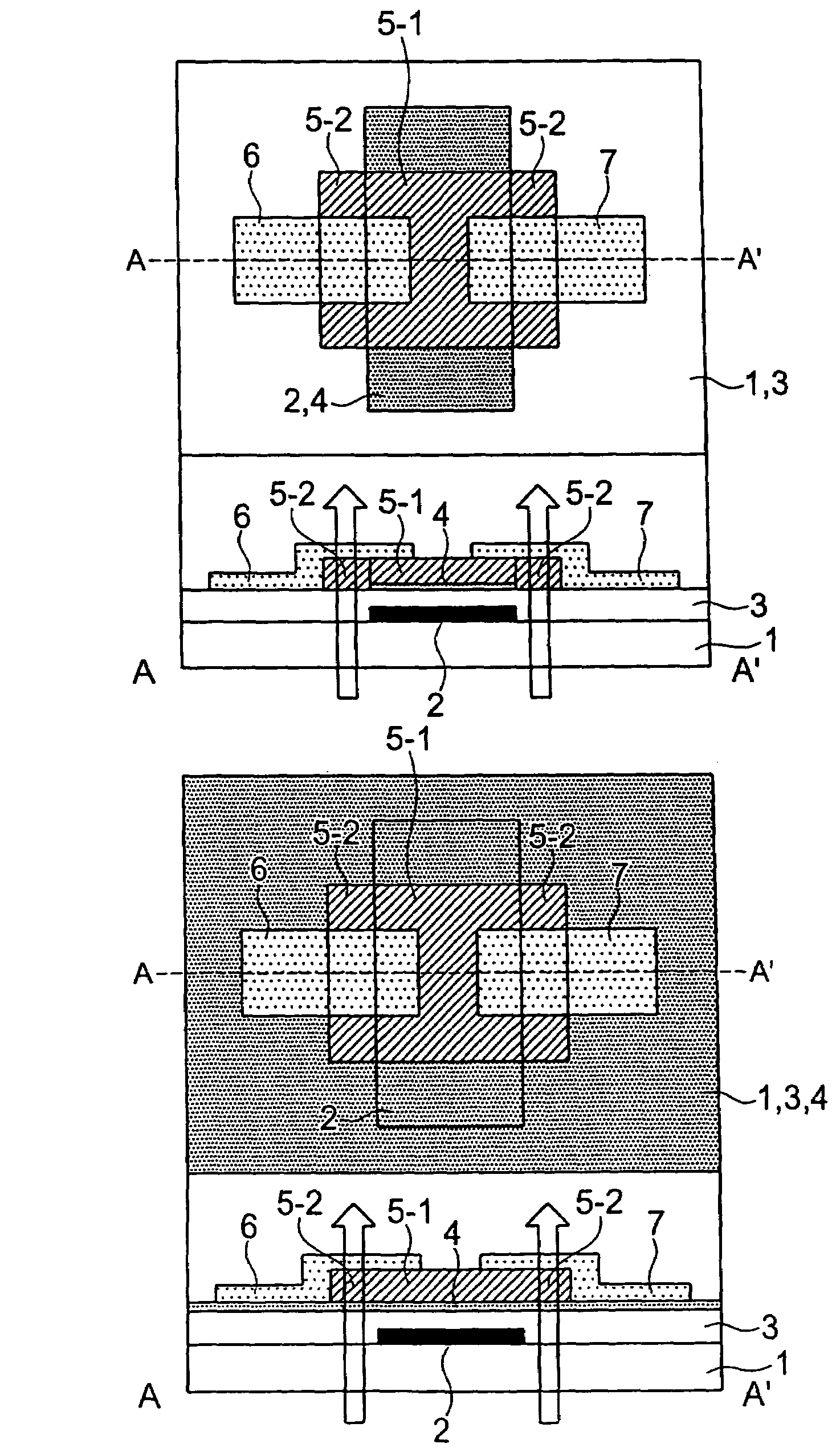
[0035]FIG. 1 is a plan view and a sectional view of the thin film transistor which is an embodiment of the present invention. The figure is a plan view of the thin film transistor and a sectional view (FIG. 1(a)) taken along a straight line A–A′ in the plan view, in comparison with the prior art (FIG. 1(b)). On a substrate 1 of Corning 1737 or a quartz, a gate electrode 2 of Cr with a film thickness of 140 nm and an insulation film 3 of a silicon oxide film with a thickness of 400 nm are sequentially stacked. Then, a self assembled monolayer film 4 of octadecyl trichlorosilane (OTS) having an approximately same pattern shape as a gate electrode is disposed in a gate electrode-projected region on the surface of the insulation film and an organic semiconductor film 5 of pentacene which is representative of organic semiconductor molecules of low molecular type, is stacked further thereon. Here, the portion of the organic semiconductor film disposed in the gate electrode region is denot...

embodiment 2

[0064]FIG. 9 is a plan view and a sectional view of the thin film transistor which is the second embodiment of the present invention. In this embodiment, drain / source electrodes 6 and 7 are formed by applying and burning an electroconductive ink made of a liquid material containing at least one of metallic microparticles, a metallic complex or an electroconductive polymer, with the use of a so-called bottom contact structure of forming an organic semiconductor film 5 after forming the drain / source electrodes 6 and 7. For the electroconductivity ink is required such a property that the ink applied outside a gate electrode-projected region, while being repelled by the liquid repellency of a SAM 4, does not infiltrate into the gate electrode-projected region, and the ink has only to be a liquid material showing adequately low resistance value after being baked. Particular examples of these materials employed include a solution in which metallic ultra-fine particles with diameters of 10...

embodiment 3

[0066]FIG. 10 is a plan view and a sectional view of the thin film transistor which is the third embodiment of the present invention. The present embodiment shows an example of forming an insulation film 3 in the thin film transistor of the embodiment 2, by anodically oxidizing a gate electrode. The gate electrode 2 is formed by forming a metallic thin film with a thickness of 200 nm made of Ta or Al on a glass substrate 1 with DC magnetron sputtering, and then processing it with photolithography. The insulator film 3 made of an oxide film with a thickness of 400 nm is formed with anodic oxidation in which DC voltage is applied. On the insulation film 3, drain / source electrodes 6 and 7 are formed self-aligned with the gate electrode 2 by forming selectively a SAM 4 in a gate electrode-projected region with the method described in the embodiment 1, and by employing a process of coating the material similar to the embodiment 2. Finally an organic semiconductor film 5 is formed in a si...


PUM

PropertyMeasurementUnit
temperatureaaaaaaaaaa
thicknessaaaaaaaaaa
thicknessaaaaaaaaaa

Abstract

The present method prevents malfunctions in switching caused by a light leakage current in an active matrix type thin film transistor substrate for a liquid crystal display and prevents display failures, by selectively disposing a self assembled monolayer film in a gate electrode-projected region of the surface of an insulator film with high definition, and by selectively improving the orientation order of an organic semiconductor film only in the gate electrode-projected region without improving the order at an irradiated portion with light outside the gate electrode-projected region.

Description

[0001]This is a continuation of application Ser. No. 10 / 786,888 filed Feb. 25, 2004 now U.S. Pat. No. 6,828,582, which application is hereby incorporated by reference in its entirety.BACKGROUND OF THE INVENTION[0002]The present invention relates to a thin film transistor with the use of a semiconductor film made of an aggregate of organic semiconductor molecules, and a manufacturing method therefor, particularly the thin film transistor characterized by having a controlled pattern shape of an electrode by improving an orientation order of the organic semiconductor molecules making up a semiconductor film with the use of a selectively disposed self assembled monolayer film, a manufacturing method therefor, and a visual display unit using it.[0003]Recently, an active matrix type display unit using an active device represented by a thin film transistor (TFT) expands its market, while being used for not only a notebook-sized personal computer or a mobile telephone but also a monitor of ...

Claims


Application Information

Patent Timeline
Patent Type & Authority Patents(United States)
IPC IPC(8): H01L35/24H01L21/4763H01L51/05H01L21/336H01L29/786H01L51/00H01L51/30H01L51/40
CPCB82Y10/00B82Y30/00H01L51/0012H01L51/0021H01L51/0533H01L51/0545H01L51/0023H01L51/0036H01L51/0039H10K71/191H10K71/621H10K71/60H10K85/115H10K85/113H10K10/476H10K10/466
Inventor ANDO, MASAHIKOWAKAGI, MASATOSHISASAKI, HIROSHI
Owner HITACHI LTD
Why Eureka
Try Eureka