Voltage modulated driver circuits for electro-optic displays

a driver circuit and electro-optic display technology, applied in the field of electro-optic displays, can solve the problems of increasing the manufacturing requiring a large number of transistors for implementation, and increasing the cost of the display, so as to achieve faster design time, lower complexity, and reduce the cost of implementation.

Active Publication Date: 2007-04-10
E INK CORPORATION
View PDF90 Cites 445 Cited by
  • Summary
  • Abstract
  • Description
  • Claims
  • Application Information

AI Technical Summary

Benefits of technology

[0020]The invention can provide, for example, lower cost of implementation for column driver circuits, faster design time and lower complexity, to decrease time-to-market and development risk. Smaller die size of integrated circuits (ICs) can decrease cost and increase yield. Smaller dice on a polycrystalline silicon panel can permit, for example, fabrication of more panels on a glass substrate or increase the fraction of panel footprint available for pixels.
[0021]In one embodiment of the invention, the number of transistors required to implement a power rail switching scheme is less than the number of transistors required to implement a conventional R-DAC system. The number of transistors can be further reduced when the number of voltage levels provided by the driver circuit is relatively low (for example, approximately 16 or fewer.) When the transistors are operated only in saturation mode, and no sensitive analog nodes exist in the circuit, a driver design can produce more accurate output levels, and can be less complex and easier to design, analyze, fabricate, and test.

Problems solved by technology

Although a DAC-based architecture has many benefits, it typically requires a large number of transistors for implementation.
This can lead to two problems: 1) the implementation of the circuit can be complex with care required to insure proper functionality and accuracy; and 2) a large area of active circuit can be required, which can lead to higher cost (especially at higher voltages.)
The cost of a large number of DACs in a high-resolution display may increase the manufacturing cost of a display.
Specialized processes may reduce the number of vendors available with a suitable manufacturing capability and may increase final cost as well as the complexity and cost of designing the architecture.

Method used


Image

  • Voltage modulated driver circuits for electro-optic displays
  • Voltage modulated driver circuits for electro-optic displays
  • Voltage modulated driver circuits for electro-optic displays

Examples


Embodiment Construction

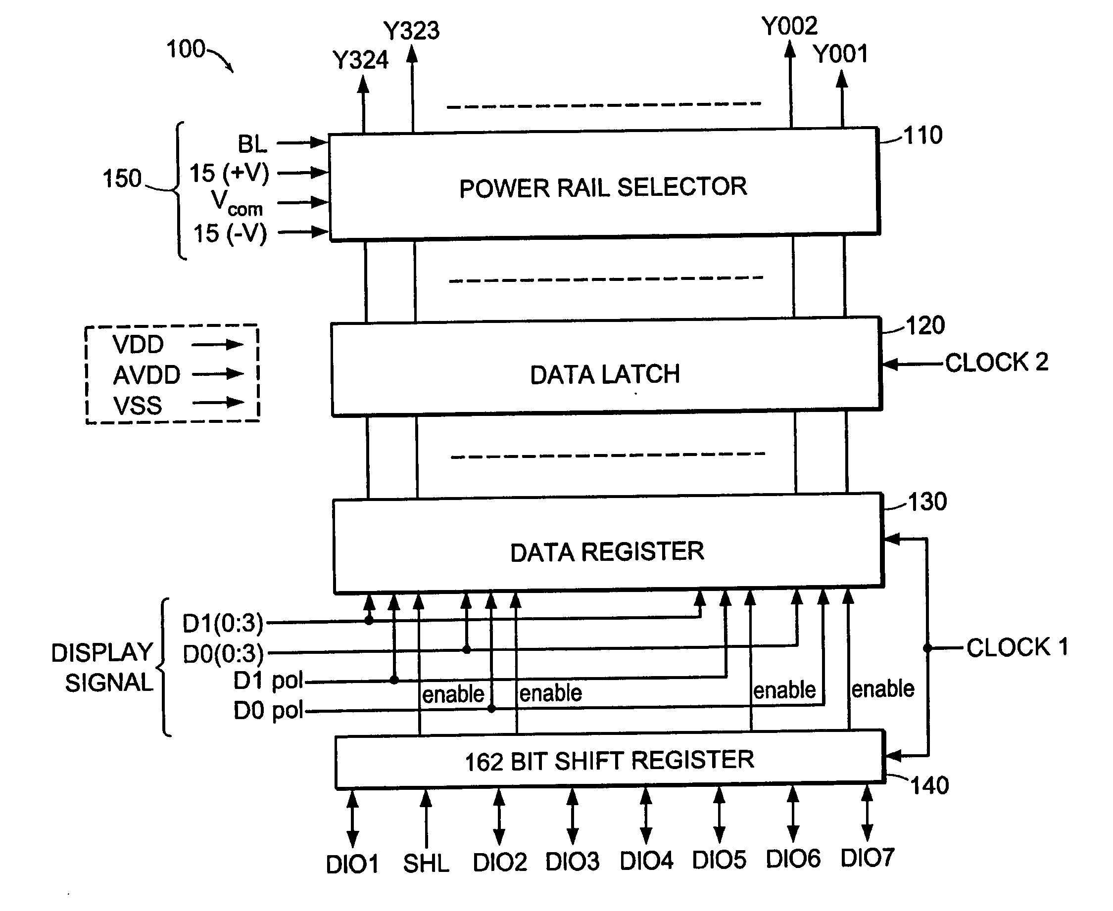
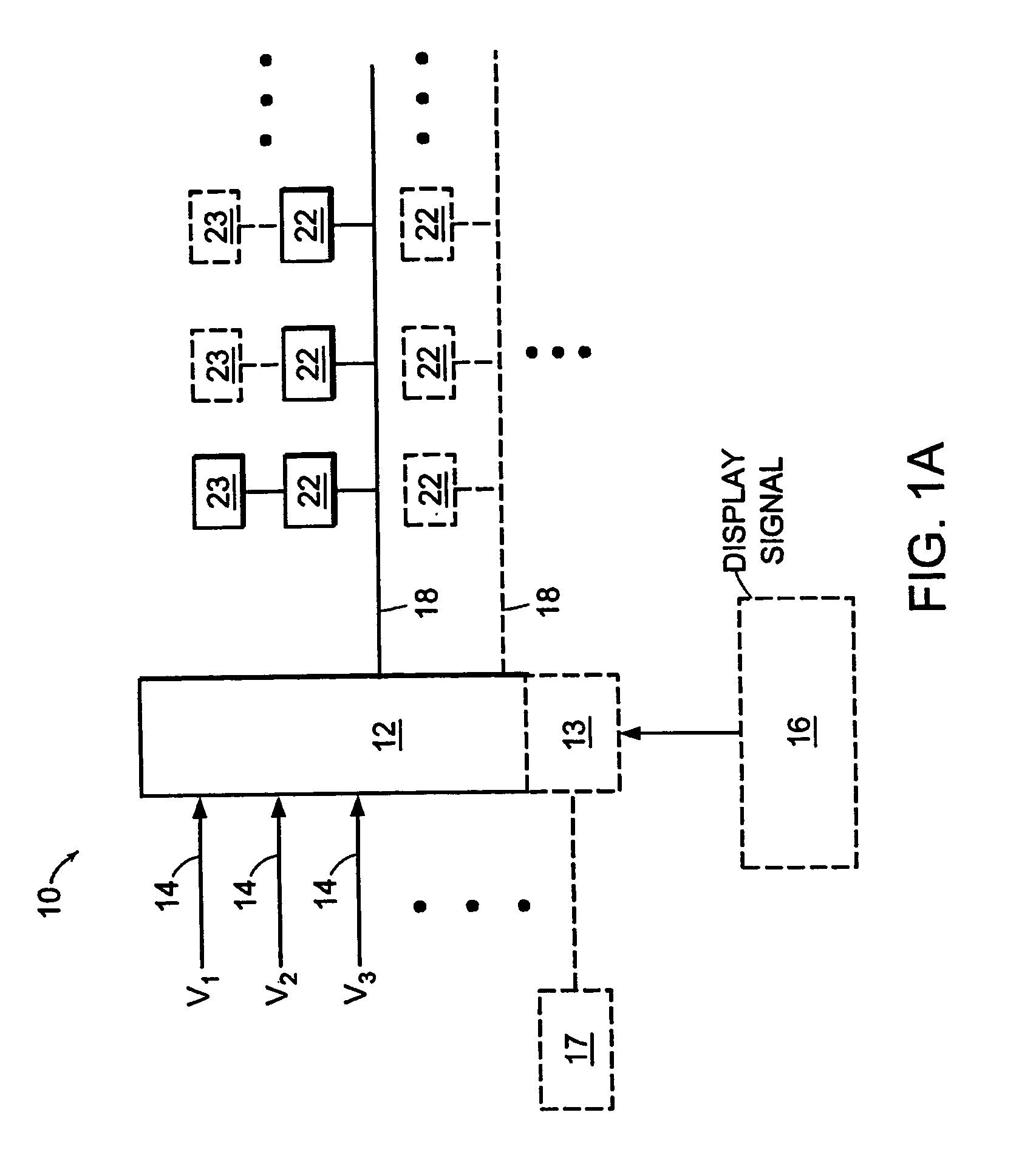
[0036]FIG. 1a is a schematic diagram of an embodiment of an addressing structure 10 of a display, according to principles of the invention. The display includes one or pairs of switch circuits 22 and pixel electrodes 23, which may be arranged in one or more columns and one or more rows. The addressing structure 10 includes a switch unit 12 that responds to a display signal, and one or more voltage sources 14 that are each associated with a voltage level V1, V2, V3—at least two of which are preferably different—and are in electrical communication with the switch unit 12. If the display includes a column of switch circuits 22, the structure 10 may include a column electrode 18 electrically connecting the switch unit 12 to each of the switch circuits 22 in the column.

[0037]The addressing structure 10 may also include a display signal generator 16 that provides the display signal. The structure may include a column voltage selector 13 to control the switch unit 12 in response to the dis...


PUM

PropertyMeasurementUnit
voltageaaaaaaaaaa
diametersaaaaaaaaaa
particle sizeaaaaaaaaaa

Abstract

A method and system for applying addressing voltages to pixels of a display involves receiving input data. The input data includes an indication of an addressing voltage impulse to be applied to a pixel via an electrode. One or more voltage sources are selected, to provide the addressing voltage impulse. The one or more voltage sources each have a pre-selected voltage. The selected one or more voltage sources are electrically connected to an electrode to apply the addressing voltage impulse to the pixel.

Description

CROSS-REFERENCE TO RELATED APPLICATIONS[0001]This application claims the benefit of U.S. Provisional Patent application Ser. No. 60 / 392,245, filed Jun. 28, 2002, the entire contents of which is herein incorporated by reference.FIELD OF THE INVENTION[0002]The present invention relates generally to electro-optic displays, and, more particularly, to methods and apparatus for active matrix addressing of such displays.BACKGROUND OF THE INVENTION[0003]Bistable or multi-stable particle-based electrophoretic displays, and other electro-optic displays, have an optical behavior that is distinct from the optical behavior of conventional liquid crystal displays (“LCDs”). Twisted nematic liquid crystals, for example, act as instantaneous voltage transducers, so that applying a given electric field to the liquid crystal display medium produces a specific gray level in response to the applied voltage, regardless of the gray level previously present at the pixel.[0004]Further, LCDs are only driven ...

Claims


Application Information

Patent Timeline
Patent Type & Authority Patents(United States)
IPC IPC(8): G09G3/36G02F1/167G09G3/20G09G3/34
CPCG09G3/344G02F1/167G09G3/2014G09G3/2022G09G3/2077G09G3/2081G09G2300/08G09G2310/0254G09G2310/027G09G2330/028G09G2340/0428G09G2340/16
Inventor GATES, HOLLY G.
Owner E INK CORPORATION
Why Eureka
Try Eureka