Liquid crystal display device and method of manufacturing the same comprising a plurality of seal patterns between a plurality of supporting patterns and a plurality of compensating patterns disposed below and aligned with the plurality of supporting patterns

a liquid crystal display and sealing pattern technology, applied in non-linear optics, instruments, optics, etc., can solve the problems of large amount of sealing material consumption and difficulty in use on a large substrate, and achieve the effects of reducing manufacturing costs, preventing bubbles, and prolonging the life of printing apparatus

Active Publication Date: 2007-04-10
LG DISPLAY CO LTD
View PDF10 Cites 23 Cited by
  • Summary
  • Abstract
  • Description
  • Claims
  • Application Information

AI Technical Summary

Benefits of technology

[0031]An object of the invention is to provide a liquid crystal display device including a seal pattern that prevents bubbles and lengthens the life span of a printing apparatus for the seal pattern.
[0032]Another object of the invention is to provide a method of manufacturing a liquid crystal display device including a seal pattern that reduces manufacturing costs.

Problems solved by technology

The screen-printing method finds wide use due to its convenience, but it is difficult to use on a large substrate.
Additionally, the dispensing method applies sealing material onto an entire surface of the screen, followed by scrubbing by the squeegee, and a large amount of sealing material may therefore be consumed.

Method used


Image

  • Liquid crystal display device and method of manufacturing the same comprising a plurality of seal patterns between a plurality of supporting patterns and a plurality of compensating patterns disposed below and aligned with the plurality of supporting patterns
  • Liquid crystal display device and method of manufacturing the same comprising a plurality of seal patterns between a plurality of supporting patterns and a plurality of compensating patterns disposed below and aligned with the plurality of supporting patterns
  • Liquid crystal display device and method of manufacturing the same comprising a plurality of seal patterns between a plurality of supporting patterns and a plurality of compensating patterns disposed below and aligned with the plurality of supporting patterns

Examples


first embodiment

[0055]FIG. 5 shows a cross-sectional view of a liquid crystal display device according to the invention. The liquid crystal display device may have an in-plane switching (IPS) mode, in which a pixel electrode and a common electrode are formed over the same substrate, and an electric field parallel to the substrate drives the liquid crystal molecules. For example, two electrodes are formed over an array substrate including a thin film transistor, and no electrode is formed over a color filter substrate. Generally, the seal pattern is formed over the color filter substrate, and thus in the IPS mode liquid crystal display device, the seal pattern may be formed over the substrate without an electrode.

[0056]FIG. 5 shows first and second substrates 210 and 230 disposed to face each other. A display region H and a seal pattern region I, which surrounds the display region H, are defined over the first and second substrates 210 and 230.

[0057]An array element layer A1 is formed over inner sur...

second embodiment

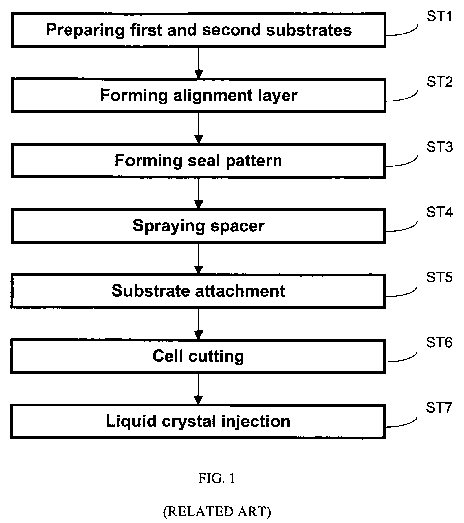
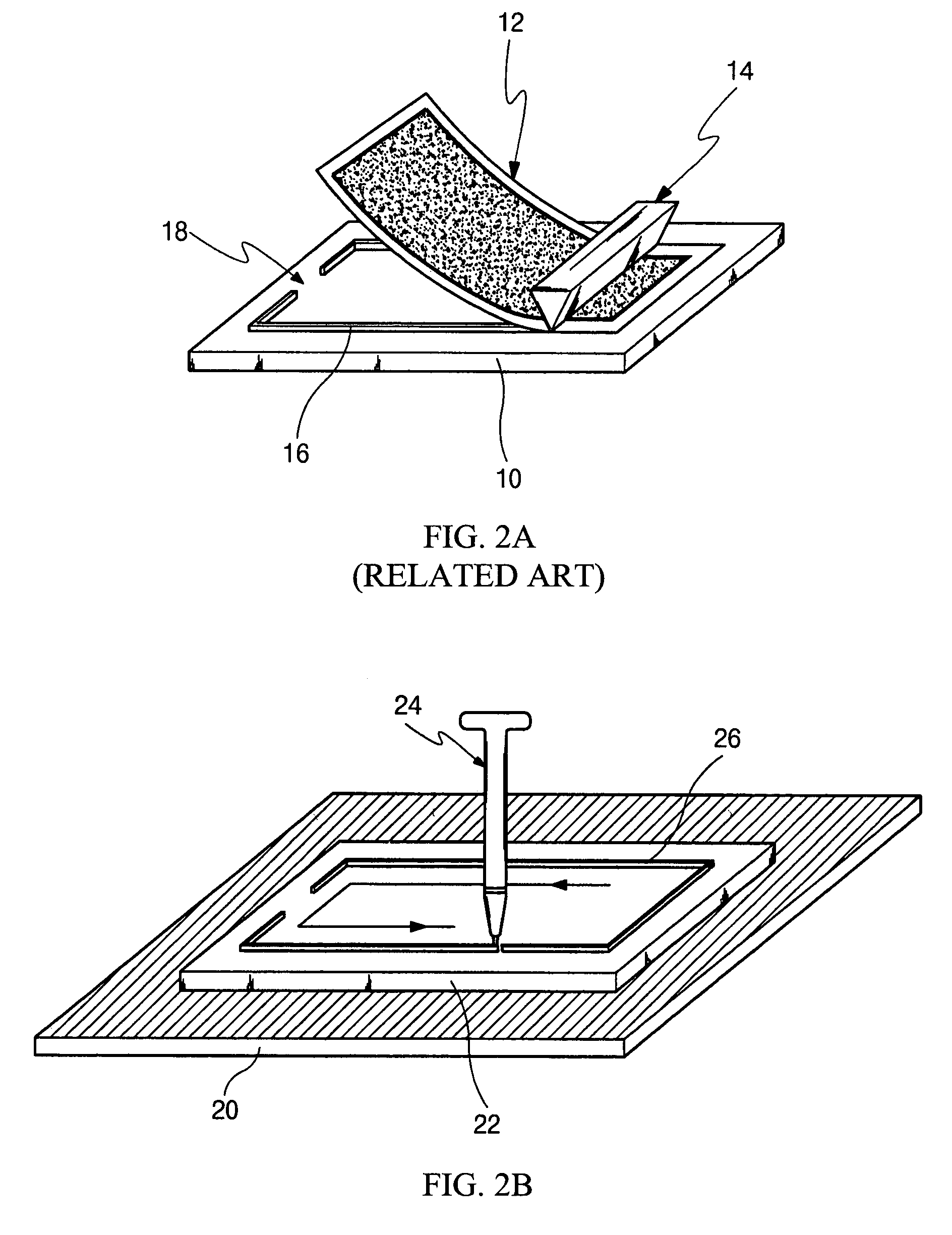
[0067]FIGS. 7A to 7D show cross-sectional views of manufacturing processes of the liquid crystal display device according to the

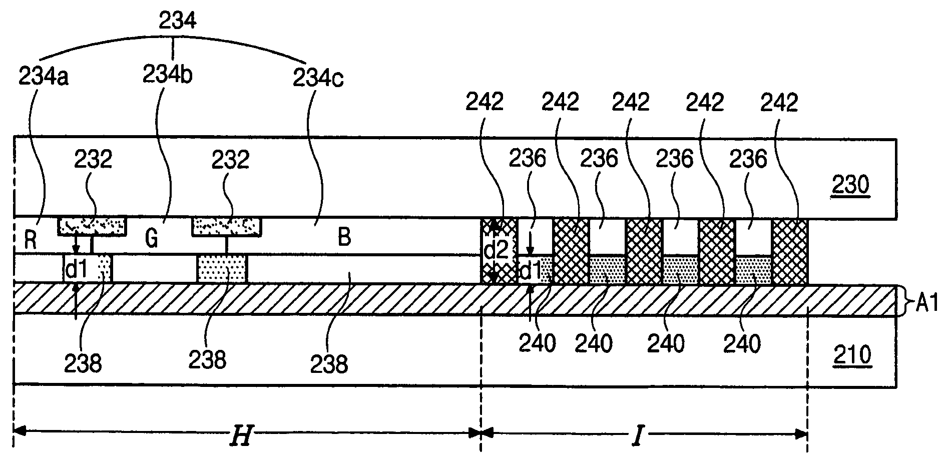
[0068]In FIG. 7A, a black matrix 432 is formed over a substrate 430 and is disposed in a display region H. A color filter layer 434 is formed over the black matrix 432 in the display region H, and a plurality of step-compensating patterns 436 are formed in a seal pattern region I, which surrounds the display region H. The color filter layer 434 includes sequentially arranged red (R), green (G) and blue (B) sub-color filters 434a, 434b and 434c. The plurality of step-compensating patterns 436 are formed of the same material and through the same process as the color filter layer 434, and the step-compensating patterns 436 are spaced apart from each other. A conductive material is formed over an entire surface of the substrate 430 including the color filter layer 434 and the step-compensating patterns 436 without a patterning process to form a common electrode...


PUM

PropertyMeasurementUnit
conductiveaaaaaaaaaa
thicknessaaaaaaaaaa
thicknessesaaaaaaaaaa

Abstract

A liquid crystal display device includes a first substrate having a first region and a second region, wherein the second region surrounds the first region, a plurality of patterned spacers over the first substrate in the first region, a plurality of supporting patterns spaced apart from each other over the first substrate in the second region, a seal pattern in the second region including the plurality of supporting patterns, a second substrate spaced apart from and attached to the first substrate by the seal pattern, and a liquid crystal layer between the first and second substrates.

Description

[0001]This application claims the benefit of Korean Patent Application No. 2003-31807, filed on May 20, 2003 in Korea, which is hereby incorporated by reference.BACKGROUND OF THE INVENTION[0002]1. Field of the Invention[0003]The invention relates to a liquid crystal display (LCD) device and more particularly, to a liquid crystal display device having an improved seal pattern and a method of manufacturing the same.[0004]2. Discussion of the Related Art[0005]Liquid crystal display (LCD) devices are image display devices that utilize the tendency of liquid crystal molecules to align according to an applied voltage. The LCD devices generally include an upper substrate upon which a color filter is formed, a lower substrate upon which a plurality of thin film transistors are formed, and a liquid crystal layer interposed between the upper and lower substrates. The LCD devices display images by controlling changing orientations of the liquid crystal molecules by applying voltage pulses to p...

Claims


Application Information

Patent Timeline
Patent Type & Authority Patents(United States)
IPC IPC(8): G02F1/1339G02F1/1335
CPCG02F1/1339G02F1/133514G02F1/13394
Inventor CHUNG, HYUN-SANGPARK, YOUNG-SUK
Owner LG DISPLAY CO LTD
Why Eureka
Try Eureka