Stacked piezoelectric element, production method thereof and electrically conducting adhesive

a piezoelectric element and production method technology, applied in the direction of generators/motors, mechanical equipment, machines/engines, etc., can solve the problems of low stress relief layer, easy cracks in the stress relief layer, and failure of electric conduction, so as to prevent separation or the like, improve elasticity, and easily undergo elastic deformation

Inactive Publication Date: 2007-04-17
DENSO CORP
View PDF4 Cites 15 Cited by
  • Summary
  • Abstract
  • Description
  • Claims
  • Application Information

AI Technical Summary

Benefits of technology

[0013]That is, at the driving of the stacked piezoelectric element, the electrically conducting adhesive layer is forming or forms a void between the microparticle and the base resin. By virtue of this void, the electrically conducting agent layer can be improved in elasticity and can readily undergo elastic deformation, so that the stress generated due to displacement of the piezoelectric layer can be satisfactorily relieved and cracking, separation or the like can be prevented from occurring.
[0014]In this way, according to the present invention, an excellent electrically conducting adhesive layer as described above is provided and therefore, a stacked piezoelectric element having excellent reliability and durability and capable of maintaining the initial performance over the long-time use can be provided.
[0023]At the driving of the stacked piezoelectric element obtained through these steps, a void is formed or can be formed between the microparticle and the base resin in the electrically conducting adhesive. By virtue of this void, the electrically conducting agent layer can be improved in elasticity and can readily undergo elastic deformation, so that the stress generated due to displacement of the piezoelectric layer can be satisfactorily relieved and cracking, separation or the like can be prevented from occurring.
[0024]In this way, according to the production method of the present invention, a stacked piezoelectric element having excellent reliability and durability and capable of maintaining the initial performance over a long time can be provided.
[0029]Accordingly, when this electrically conducting adhesive is used by bonding and curing it on an apparatus undergoing displacement during driving, such as a stacked piezoelectric element, a void is formed or can be formed between a microparticle and the base resin. By virtue of this void, the electrically conducting adhesive after curing can be improved in elasticity and can readily undergo elastic deformation, so that the stress generated due to displacement of the piezoelectric layer can be satisfactorily relieved and cracking, separation or the like can be prevented from occurring.
[0030]In this way, the electrically conducting adhesive of the present invention can provide, when applied as an electrically conducting material, an apparatus having enhanced reliability and durability and capable of maintaining its initial performance over a long time.

Problems solved by technology

In such a stacked piezoelectric element, an electrically conducting adhesive having flexibility is used to cope with the displacement of the piezoelectric layer generated during driving but, as the stacked piezoelectric element is used for a long time at a high temperature, troubles such as cracking or separation occur in the electrically conducting adhesive due to displacement of the piezoelectric layer or thermal curing of the resin, and this gives rise to a problem that electrical conduction failure occurs.
However, the strength of the stress-relieving layer is low and therefore, cracks readily occur in the stress-relieving layer.
Also, the joined portion between the stress-relieving layer and the take-out electrode is insufficient in adhesion and readily causes separation.
However, in this method, similarly to the above, troubles such as cracking or separation occur due to thermal curing or the like of the resin.

Method used


Image

  • Stacked piezoelectric element, production method thereof and electrically conducting adhesive
  • Stacked piezoelectric element, production method thereof and electrically conducting adhesive
  • Stacked piezoelectric element, production method thereof and electrically conducting adhesive

Examples


example 1

[0080]The stacked piezoelectric element according to Examples of the present invention is described by referring to FIGS. 1 to 3.

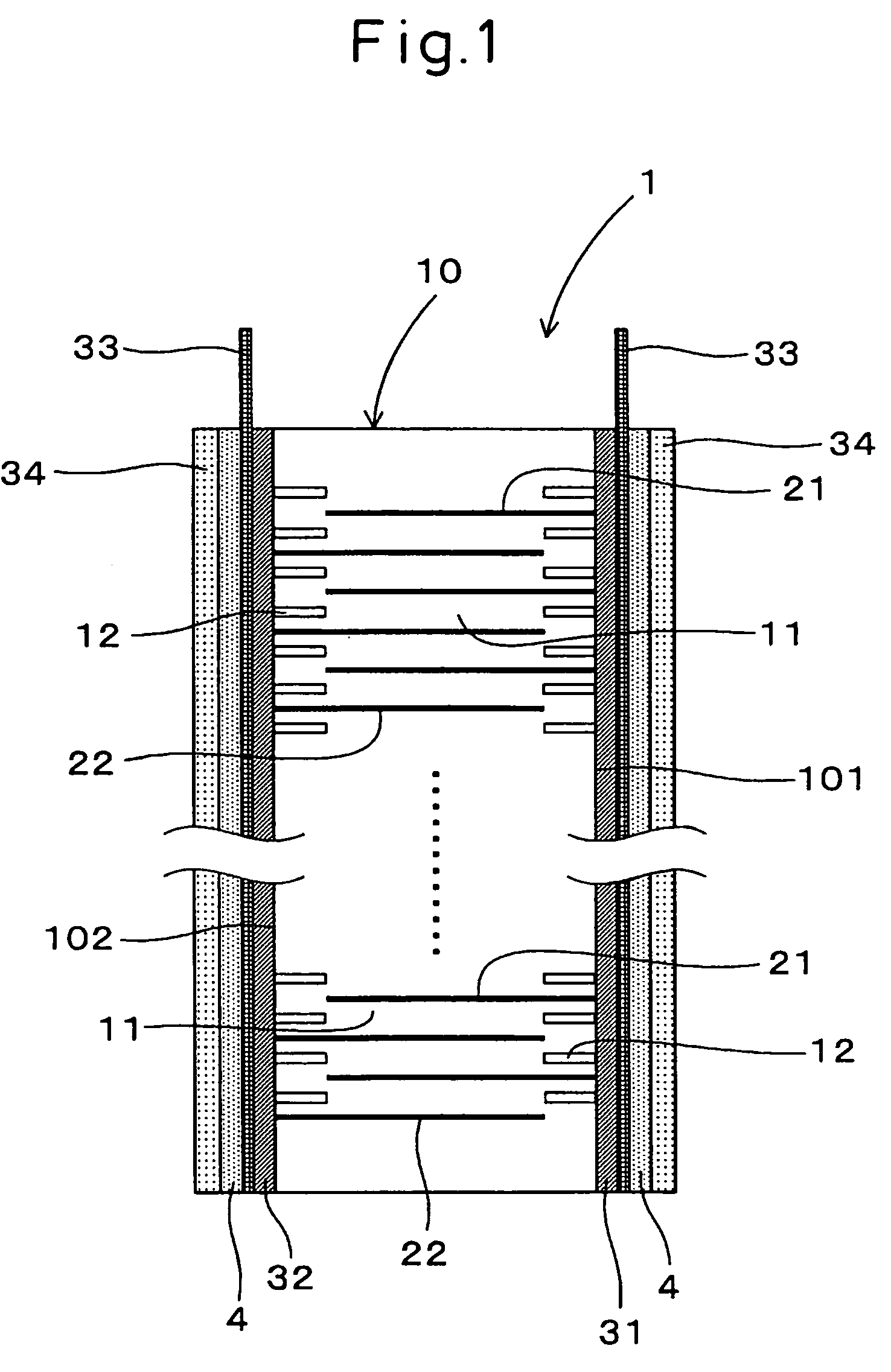
[0081]The stacked piezoelectric element 1 of the present invention comprises, as shown in FIG. 1, a ceramic stack 10 obtained by alternately stacking a piezoelectric layer 11 comprising a piezoelectric material and an internal electrode layer 21 (22) having electrical conductivity, and an electrically conducting adhesive layer 4 provided to allow for electrical conduction of the internal electrode layer 21 (22) of the same polarity on the side surface of the ceramic stack 10.

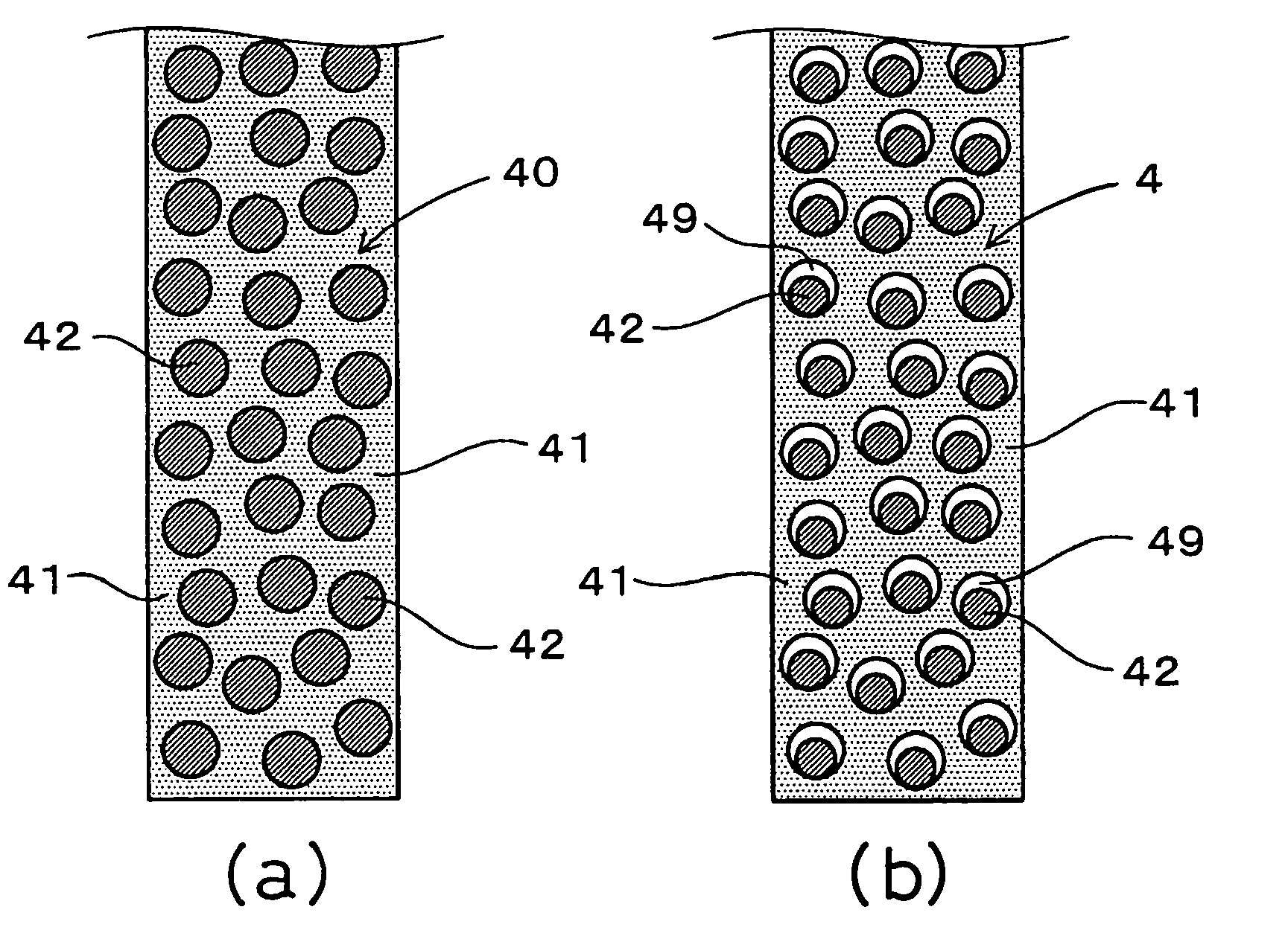
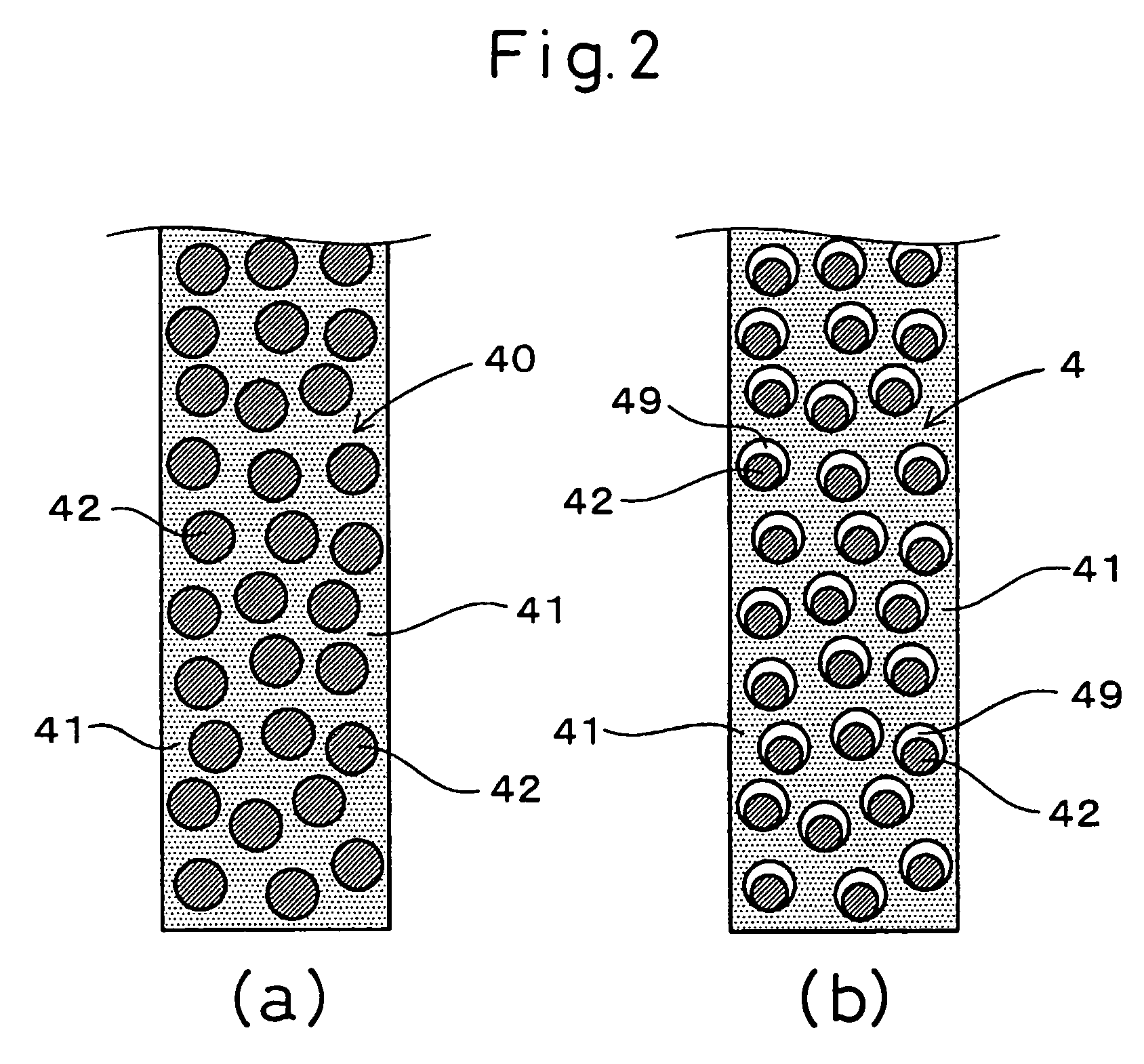
[0082]The electrically conducting adhesive layer 4 comprises, as shown in FIG. 2(b), a base resin 41 having dispersed therein an electrically conducting filler (not shown) and microparticles 42.

[0083]The boundary between the microparticle 42 and the base resin 41 is in a state that a void 49 is formed at least in a part between those two members.

[0084]This is described in detail below....

example 2

[0135]This Example is a case where, in the stacked piezoelectric element 1 of Example 1, the electrically conducting adhesive 40 contains, as the microparticle 42, a particle with at least the surface thereof having a non-adhesive surface 429 capable of not adhering to said base resin 41.

[0136]In this Example, silicone was used as the microparticle 42. Other than silicone, for example, Teflon (registered trademark) may be used.

[0137]Others were the same as in Example 1.

[0138]In this Example, an electrically conducting adhesive containing, as the microparticle 42, a particle with at least the surface thereof having a non-adhesive surface 429 capable of not adhering to said base resin 41 was used.

[0139]In the electrically conducting adhesive layer 4, after the curing step, as shown in FIG. 7(a), as the surface of the microparticle 42 has a non-adhesive surface 429 capable of not adhering to the base resin 41, the microparticle 42 does not adhere to the base resin 41 and these two memb...

example 3

[0142]This Example is a case where, in the stacked piezoelectric element 1 of Example 1, as shown in FIG. 8, the electrically conducting adhesive 40 uses, as the microparticle 42, a particle comprising a particle body 421 and an exterior non-adhesive coat layer 422 covering the particle body surface and forming the non-adhesive surface 429.

[0143]In this Example, a resin particle was used as the particle body 421 of the microparticle 42. Other than this, for example, a ceramic particle or a glass particle may be used.

[0144]Also, silicone was used as the exterior non-adhesive coat layer 422. Other than silicone, for example, Teflon (registered trademark) may be used.

[0145]Others were the same as in Example 1.

[0146]In this Example, a particle comprising a particle body 421 and an exterior non-adhesive coat layer 422 covering the particle body surface and forming the non-adhesive surface 429 was used as the microparticle 42.

[0147]Therefore, in the electrically conducting adhesive layer ...


PUM

PropertyMeasurementUnit
particle diameteraaaaaaaaaa
thicknessaaaaaaaaaa
thicknessaaaaaaaaaa

Abstract

An object of the present invention is to provide a stacked piezoelectric element with excellent reliability and durability, a production method thereof and an electrically conducting adhesive.A stacked piezoelectric element comprising a ceramic stack obtained by alternately stacking a piezoelectric layer comprising a piezoelectric material and an internal electrode layer having electrical conductivity, and an electrically conducting adhesive layer provided to allow for electrical conduction to said internal electrode layer of the same polarity on the side surface of said ceramic stack,wherein said electrically conducting adhesive layer comprises a base resin having dispersed therein an electrically conducting filler and microparticles, andthe boundary between said microparticle and said base resin is in a state that a void is formed at least in a part between those two members or in a state that when said base resin is elongated, a void can be formed between those two members.

Description

[0001]This application is a new U.S. patent application that claims benefit of JP 2004-250926, filed 30 Aug. 2004, the entire contents of each of which are hereby incorporated by reference.FIELD OF THE INVENTION[0002]The present invention relates to a stacked piezoelectric element applied to, for example, a piezoelectric actuator and also relates to a production method thereof and an electrically conducting adhesive.BACKGROUND OF THE INVENTION[0003]A stacked piezoelectric element generally comprises a ceramic stack obtained by alternately stacking piezoelectric layers comprising a piezoelectric material and internal electrode layers having electrical conductivity, and this stacked piezoelectric element is constructed such that a pair of side surface electrodes electrically connected to respective side surfaces of the ceramic stack are provided, a pair of take-out electrodes are joined to respective side surface electrodes by using, for example, an electrically conducting adhesive co...

Claims


Application Information

Patent Timeline
Patent Type & Authority Patents(United States)
IPC IPC(8): H01L41/047H02N2/02F02M51/00F02M51/06H01B1/22H01L41/083H01L41/22H01L41/27H01L41/293
CPCH01L41/0472H01L41/0833H01L41/293H01L41/0477H10N30/872H10N30/877H10N30/503H10N30/063
Inventor KADOTANI, SHIGEIWASE, AKIO
Owner DENSO CORP
Why Eureka
Try Eureka