MRAM memory with residual write field reset

a write field and memory technology, applied in the field of magnetoresistive random access memory, can solve the problems of poor write endurance of flash memory, high voltage requirements, slow program and erase times,

Inactive Publication Date: 2007-04-17
EVERSPIN TECHNOLOGIES
View PDF10 Cites 10 Cited by
  • Summary
  • Abstract
  • Description
  • Claims
  • Application Information

AI Technical Summary

Problems solved by technology

Disadvantages of FLASH memory include high voltage requirements and slow program and erase times. Also, FLASH memory has a poor write endurance of 104–106 cycles before memory failure.
Hence, FLASH memory is limited in the dimensions to which it can be scaled.
As the lateral dimension of an MRAM device decreases, three problems occur.
First, the switching field increases for a given shape and film thickness, requiring a larger magnetic field to switch.
A major problem with having a

Method used


Image

  • MRAM memory with residual write field reset
  • MRAM memory with residual write field reset
  • MRAM memory with residual write field reset

Examples


Embodiment Construction

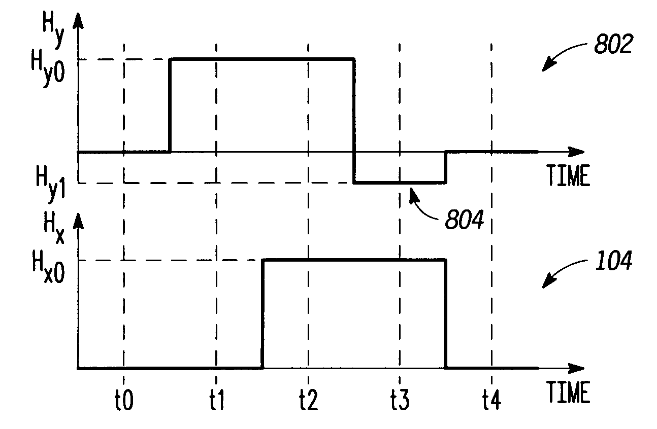
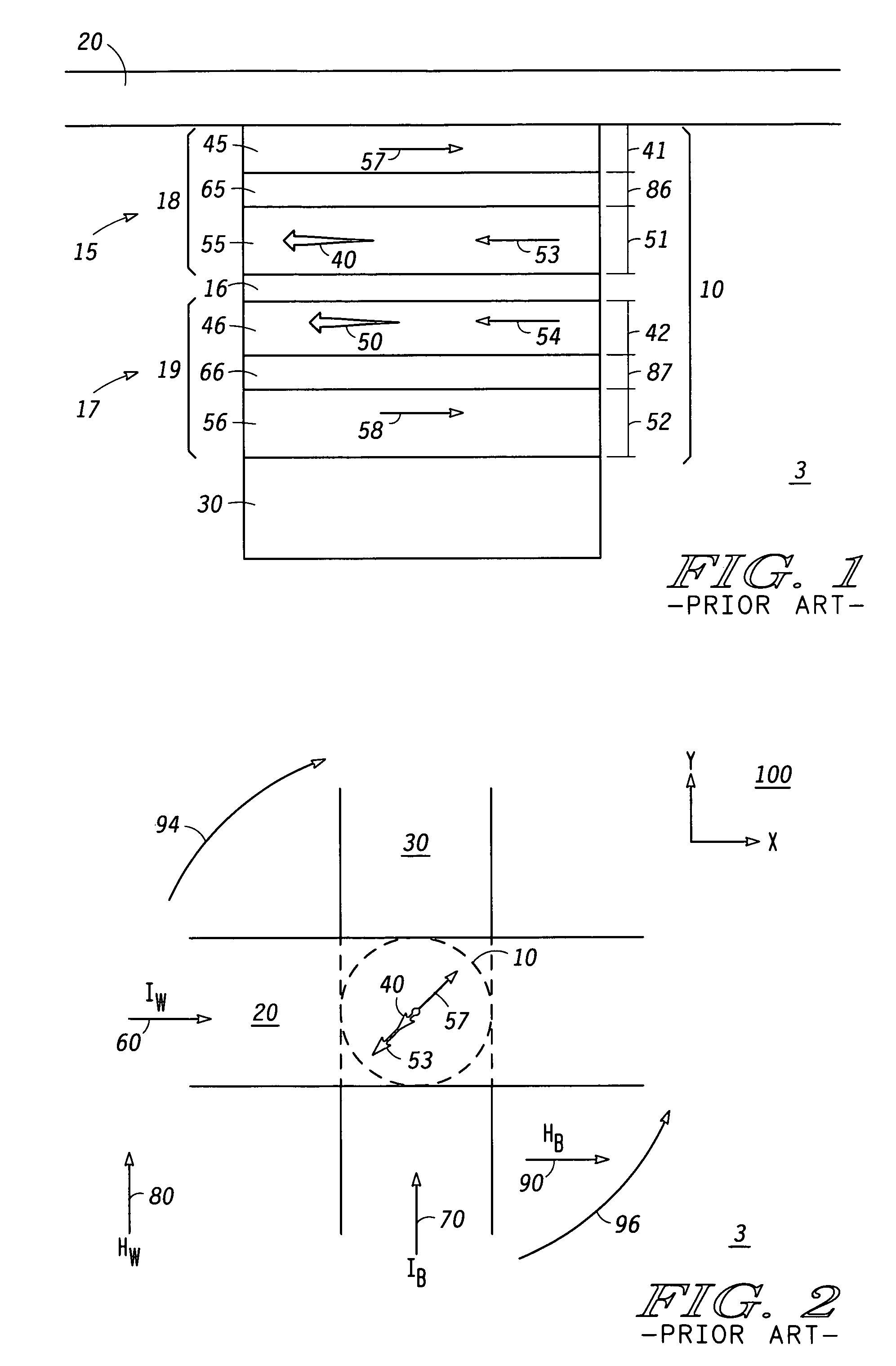
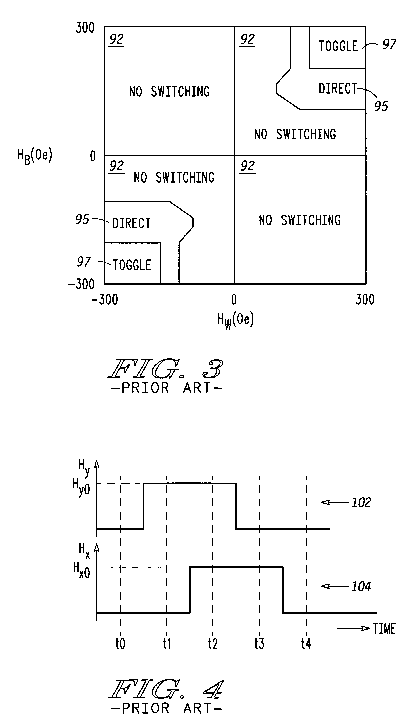
[0025]A known toggle MRAM is illustrated by Savtchenko et al. in U.S. Pat. No. 6,545,906 and functions to provide stored information in a memory cell by selectively positioning magnetic fields associated with current conducted by two perpendicular conductors. Each bit of an MRAM has a magnetic tunnel junction (MTJ) which is composed of a composite of conductive layers separated by a single insulator. Each of the conductive layers has a magnetization direction. The resistance of a memory bit is reduced when the magnetization of the conductive layers adjacent to the insulator are in a same direction. Conversely, the resistance of a memory bit is increased when the magnetization of the conductive layers adjacent to the insulator are in an opposite direction.

[0026]In order to enhance the applied magnetic field from current flowing through the two orthogonal conductors, each of the conductors has three of its outward facing surfaces lined with a ferromagnetic cladding material such as Ni...


PUM


Abstract

A magnetoresistive random access memory (MRAM) (900) that is susceptible to a residual magnetic field is compensated during a write operation. A first magnetic field (208) is applied to a memory cell during a first time period, the first magnetic field having a first direction (y) and a first magnitude. A second magnetic field (212) is applied to the memory cell during a second time period and having a second direction (x) and a second magnitude. A third magnetic field (702) is applied to the memory cell during a third time period, wherein the third time period overlaps at least a portion of the second time period, the third magnetic field having a third direction (−y) which is approximately opposite to the first direction of the first magnetic field. Currents are selectively applied through conductors in the memory cell to apply the three magnetic fields.

Description

CROSS REFERENCE TO RELATED APPLICATION[0001]This patent is related to a copending U.S. patent application Ser. No. 11 / 297,202 entitled “MRAM With A Write Driver And Method Therefor” filed of even date and assigned to the assignee of record herein.FIELD OF THE INVENTION[0002]This invention relates to Magnetoresistive Random Access Memories (MRAMs), and more particularly to architectures for MRAMs.BACKGROUND OF THE INVENTION[0003]Non-volatile memory devices, such as FLASH memories, are extremely important components in electronic systems. FLASH is a major non-volatile memory device in use today. Disadvantages of FLASH memory include high voltage requirements and slow program and erase times. Also, FLASH memory has a poor write endurance of 104–106 cycles before memory failure. In addition, to maintain reasonable data retention, the scaling of the gate oxide is restricted by the tunneling barrier seen by the electrons. Hence, FLASH memory is limited in the dimensions to which it can be...

Claims


Application Information

Patent Timeline
IPC IPC(8): G11C11/00
CPCG11C11/15
Inventor NAHAS, JOSEPH J.ANDRE, THOMAS W.SUBRAMANIAN, CHITRA K.RIZZO, NICHOLAS DAVID
Owner EVERSPIN TECHNOLOGIES
Why Eureka
Try Eureka