Switching signal modulation circuit

a technology of switching signal and modulation circuit, which is applied in the direction of pulse generator, pulse technique, instruments, etc., can solve the problems of reducing the efficiency of switching signal, and reducing the size of control circuit, so as to prevent the saturation of the transformer, reduce noise, and reduce the effect of large allowan

Active Publication Date: 2007-04-24
COSEL
View PDF6 Cites 7 Cited by
  • Summary
  • Abstract
  • Description
  • Claims
  • Application Information

AI Technical Summary

Benefits of technology

[0006]According to the present invention there is provided a switching signal modulating circuit used for PWM control that facilitates the reduction of noise by the spectrum spread, at a low cost, using a combination of multi-purpose ICs without requiring any specific circuits and parts. The present invention is configured as follows. A switching signal modulation circuit of the present invention comprises a switching control circuit having an ON time control terminal and an OFF time control terminal, the switching control circuit capable of adjusting respectively separately ON time and OFF time of a switching signal using resistance values of resistors externally attached respectively to the ON time control terminal and the OFF time control terminal; a spread signal generating circuit operable to output a spread signal; an ON time setting resistor connected between the ground and the ON time control terminal of the switching control circuit; an OFF time setting resistor connected between the ground and the OFF time control terminal of the switching control circuit; a first weight resistor operable to vary the frequency and the duty of the switching signal, the first weight resistor connected between an output of the spread signal generating circuit and the ON time control terminal of the switching control circuit; and a second weight resistor operable to vary the frequency and the duty of the switching signal, the second weight resistor connected between the output of the spread signal generating circuit and the OFF time control terminal of the switching control circuit.
[0008]The switching signal modulating circuit of the present invention uses a multi-purpose IC for PWM control such as, for example, M5199 from Mitsubishi Electric Corp., etc. as the switching control circuit and a multi-purpose timer IC such as, for example, NE555 from Signetics Co., Ltd., as the spread signal generating circuit, and determines the ON time period and the OFF time period by connecting the external resistors respectively with an ON time period control terminal and OFF time period control terminal of the switching control circuit as well as can apply a stable frequency spread having no hunting to the switching signal using a simple configuration of connecting the resistors for varying the frequency and the duty respectively between the output of the spread signal generating circuit and the ON time period control terminal, and the output of the spread signal generating circuit and the OFF time period control terminal. Furthermore, because it is not necessary to prevent the saturation of the transformer due to the spectrum spread and take a large allowance for saturation flux density, the noise can be reduced even with a small-sized transformer without making the transformer larger to reduce the noise. Yet furthermore, the duty ratio can be determined appropriately only by changing the ratios of the ON time period setting resistor and the OFF time period setting resistor in response to the spread width of the switching frequency and an inverter can be prevented from being broken by the saturation of the transformer, by reducing the duty for ON state when the switching frequency is lowered by the spread signal. In addition, because a stable and low-cost circuit can be provided and multi-purpose parts can be used, no problem concerning delivery arises. The above and other objects, features and advantages of the present invention will become more apparent from the following detailed description with reference to the drawings.

Problems solved by technology

However, such a conventional switching signal modulating circuit as above needs a peak detecting circuit and a sample holding circuit and has a problem that a transformer is saturated because the width of an ON time period is increased when the switching frequency is lowered due to the frequency spread.
Furthermore, as to the above switching signal modulating circuit, the circuitry is complicated, designing of the logic and adjustment take time and the control circuit becomes bulky.
However, this needs much time to deliver and a higher cost.
In addition, other problems also arise that the scope of the designing to reduce the spread frequency is limited by the restriction on the size of the transformer, etc.

Method used


Image

  • Switching signal modulation circuit
  • Switching signal modulation circuit
  • Switching signal modulation circuit

Examples


Embodiment Construction

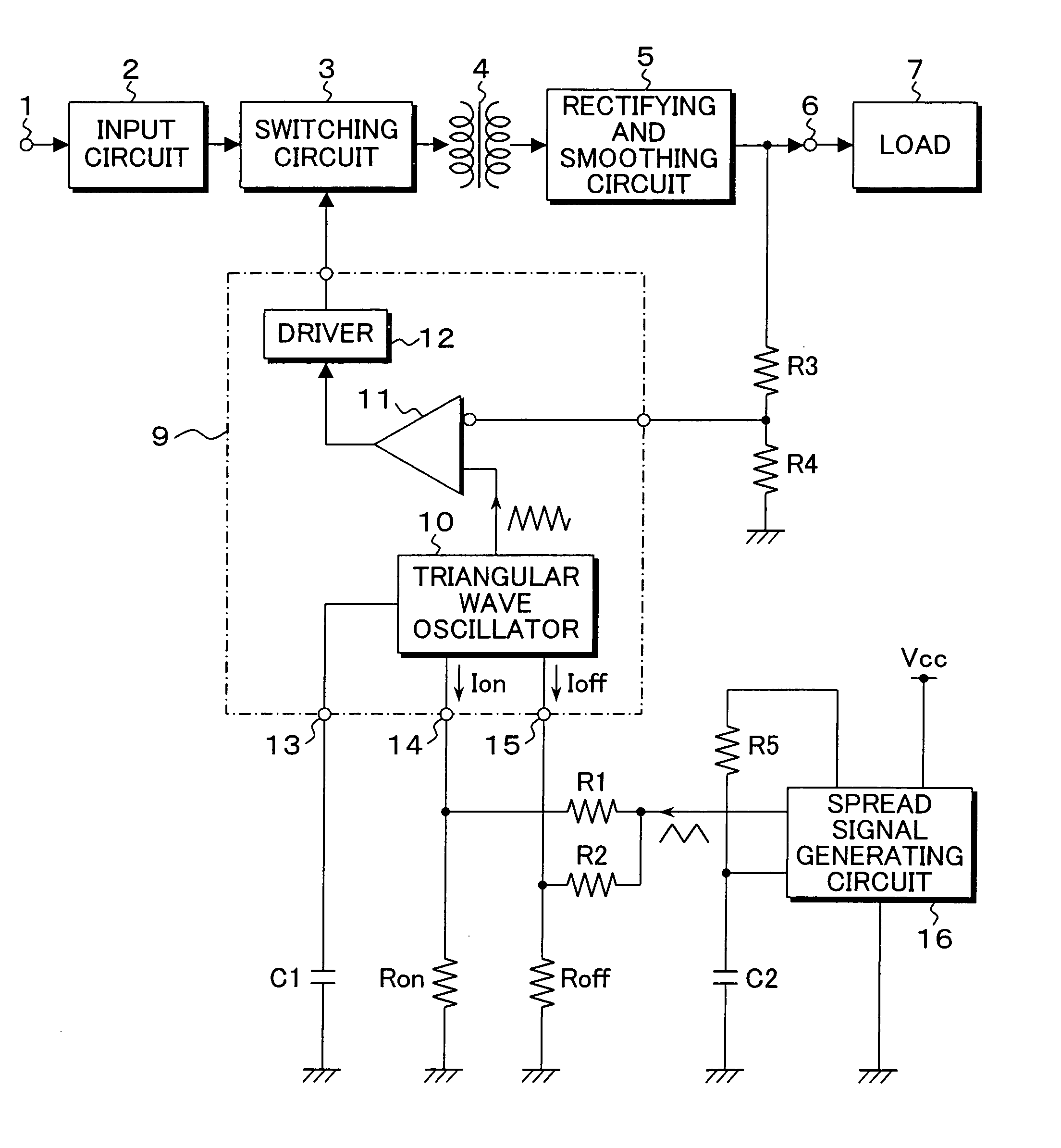
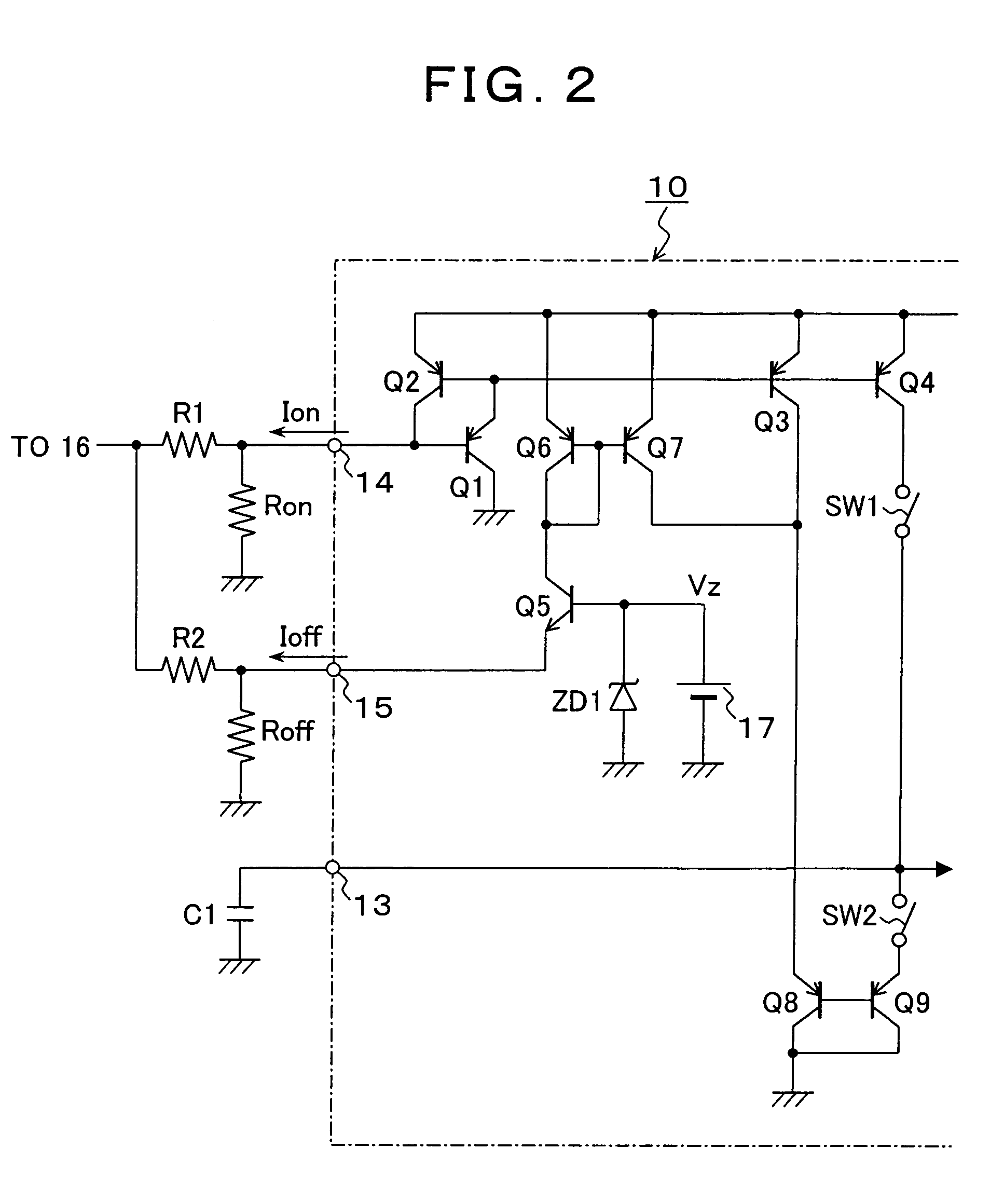
[0012]FIG. 1 is a circuit block diagram showing an embodiment of the present invention taking a example of a switching regulator. In FIG. 1, the main circuit of the switching regulator comprises an input terminal 1, an input circuit 2, a switching circuit 3, a transformer 4, a rectifying and smoothing circuit 5 and an output terminal 6, and supplies a constant DC power voltage to a load 7. The input circuit 1 is provided with a rectifying circuit and a smoothing circuit if the input circuit is of an AC input type, and with an input smoothing capacitor if the input circuit is of a DC input type. The switching circuit 3 constitutes an inverter by connecting in series a switching element such as a MOS-FET, etc. with the primary coil of the transformer 4. The rectifying circuit 5 converts the output of the secondary coil of the transformer 4 into a DC by rectifying and smoothing the output. A switching control circuit 9 is disposed on the above main circuit of the switching regulator. T...


PUM


Abstract

A switching signal modulation circuit includes a switching control circuit having an ON time control terminal and an OFF time control terminal, the switching control circuit capable of adjusting respectively separately ON time and OFF time of a switching signal using values of resistors externally attached respectively to the ON time control terminal and the OFF time control terminal; a spread signal generating circuit operable to output a spread signal; an ON time setting resistor connected between the ground and the ON time control terminal of the switching control circuit; an OFF time setting resistor connected between the ground and the OFF time control terminal of the switching control circuit; a first weight resistor operable to vary the frequency and the duty of the switching signal, the first weight resistor connected between an output of the spread signal generating circuit and the ON time control terminal of the switching control circuit; and a second weight resistor operable to vary the frequency and the duty of the switching signal, the second weight resistor connected between the output of the spread signal generating circuit and the OFF time control terminal of the switching control circuit.

Description

BACKGROUND OF THE INVENTION[0001]1. Field of the Invention[0002]The present invention relates generally to a switching signal modulating circuit for use in switching control of a switching regulator, etc., and more particularly, to a switching signal modulating circuit that varies randomly the frequency and the duty of a switching signal using a spread signal.[0003]2. Description of the Related Art[0004]Conventionally, a switching regulator is adapted to produce a control signal for frequency modulation of a triangular wave signal generating circuit by detecting the maximal value of a triangular wave signal and sampling a random signal at the timing of the detected maximal value in order to reduce the peak levels of the conduction noise and the radiation noise accompanied by switching control, is adapted to obtain a PMW signal by varying randomly the triangular signal by a spread width of 0.8 to 1.2 times as wide as that of the central frequency and by comparing this triangular sign...

Claims


Application Information

Patent Timeline
Patent Type & Authority Patents(United States)
IPC IPC(8): G05F1/40H02M3/335H02H7/00H02M3/28H03K4/06H03K7/08
CPCH02M3/28H03K4/06H02M1/44
Inventor MITSUO, NAKADA
Owner COSEL
Why Eureka
Try Eureka