Solid-state electronic image pickup apparatus and method of driving the same

a pickup apparatus and electronic technology, applied in the direction of instruments, television systems, television system scanning details, etc., can solve the problems of low shutter speed and long frame rate, and achieve the effect of reducing the frame ra

Active Publication Date: 2007-04-24
FUJIFILM CORP +1
View PDF8 Cites 18 Cited by
  • Summary
  • Abstract
  • Description
  • Claims
  • Application Information

AI Technical Summary

Benefits of technology

[0007]An object of the present invention is to reduce the frame rate.
[0008]Another object of the present invention is maintain the shutter speed (exposure time period) relatively high (short) while the flash synchronization is attained.
[0019]According to the present invention, the signal charges are successively read out at a predetermined time interval only for limited number of photoelectric conversion devices of the whole photoelectric conversion devices provided on image sensor, the frame rate can be reduced, even if there is a limit to shorten the pixel rate.
[0022]In this way, since all the specified photoelectric conversion devices are simultaneously exposed by the strobe flash in the common time period, a suitable strobe imaging can be performed. Further the number of the specified photoelectric conversion devices is less than that of the whole photoelectric conversion devices, so that the signal charge accumulation time period in the photoelectric conversion devices, i.e., the shutter speed can be relatively high.
[0027]Also in the electronic camera, the frame rate can be reduced, thereby making it possible to shorten the intervals of imaging. It is possible to prevent a problem that an imaging scene is restricted.

Problems solved by technology

As a result, the shutter speed becomes low and frame rate becomes long.

Method used


Image

  • Solid-state electronic image pickup apparatus and method of driving the same
  • Solid-state electronic image pickup apparatus and method of driving the same
  • Solid-state electronic image pickup apparatus and method of driving the same

Examples


Embodiment Construction

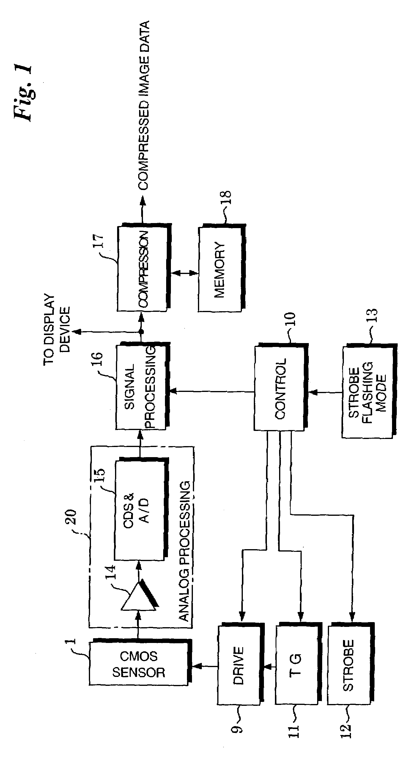
[0042]FIG. 1 is a block diagram showing a part of the electrical configuration of a digital still camera comprising a CMOS type image sensor.

[0043]The overall operation of the digital still camera is supervised by a control circuit 10.

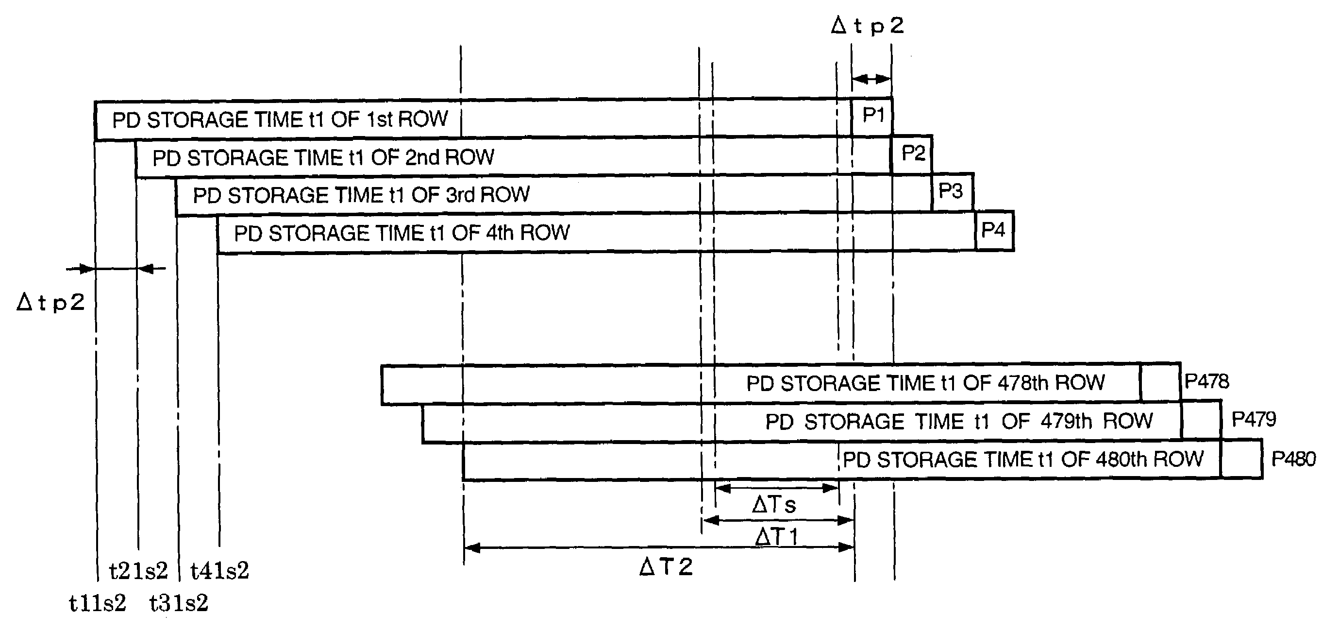
[0044]The digital still camera is provided with a strobe (electronic) flashing device 12 such that strobe (electronic) flash imaging can be performed. A strobe flashing mode is set by a strobe flashing mode switch 13 (a strobe flashing mode may be automatically set by the control circuit 10 in accordance with exposure conditions, and so on.). When a signal representing the strobe flashing mode is inputted to the control circuit 10, the control circuit 10 and the strobe flashing device 12 enter the strobe flashing mode, in which it emits light in response to the timing of imaging (the timing of strobe flashing will be described in detail later).

[0045]Various types of clock pulses are outputted from a timing generator 11, and are fed to a drive circuit 9...


PUM


Abstract

In order to reduce the frame rate, when all photodiodes contributing to output of a video signal in a CMOS image sensor must be simultaneously exposed (at the timing of strobe flashing Δts), as in a case where strobe is flashed, readout pixels composing the CMOS type image sensor are thinned such that the number of photodiodes contributing to the video signal outputted from the CMOS type image sensor is reduced. A time period Δtp2 required for processing (of the video signal caused by a row of photodiodes) in an analog processing circuit connected to the succeeding stage of the CMOS type image sensor is shortened, thereby reducing the frame rate.

Description

BACKGROUND OF THE INVENTION[0001]1. Field of the Invention[0002]The present invention relates to a solid-state electronic image pickup apparatus comprising an image sensor having a lot of photoelectric conversion devices (transducers) (pixels) arranged two dimensionally and capable of being selective readout (random access) and a method of driving the same, and an electronic camera including the solid-state electronic image pickup apparatus.[0003]2. Description of the Background Art[0004]In image sensors capable of being selective readout (such as a CMOS (Complementary Metal-Oxide Semiconductor) type and a CID (Charge Injection Device) type) as shown in FIG. 13, signal charges respectively accumulated in photoelectric conversion devices are successively outputted for each pixel (photoelectric conversion device) as a video signal corresponding to one frame. The video signal outputted from the image sensor is inputted to an analog processing circuit including an amplification circuit,...

Claims


Application Information

Patent Timeline
Patent Type & Authority Patents(United States)
IPC IPC(8): H04N5/14H01L27/00H01L31/062H04N5/222H04N5/235H04N5/341H04N5/345H04N5/353H04N5/369H04N5/3745H04N9/04
CPCH04N5/2354H04N5/3454H04N5/3456H04N5/3532H04N5/3745H04N9/045H04N23/63H04N23/74H04N25/445H04N25/443H04N25/531H04N25/70H04N25/77H04N25/134
Inventor NISHINO, NAOYUKIUCHIYAMA, HIROYUKIKOTANI, TAKAAKIKIMURA, SOICHIRO
Owner FUJIFILM CORP
Why Eureka
Try Eureka