Magnetic memory device and method of reading the same

a memory device and magnetic technology, applied in semiconductor devices, digital storage, instruments, etc., can solve the problems of inability difficult to improve storage capacity and access speed, and inability to ignore the noise of variations, etc., to achieve excellent operation stability, less power consumption, and high reliability

Active Publication Date: 2007-04-24
TDK CORPARATION
View PDF24 Cites 15 Cited by
  • Summary
  • Abstract
  • Description
  • Claims
  • Application Information

AI Technical Summary

Benefits of technology

[0022]The present invention has been achieved in consideration of the problems and an object of the invention is to provide a magnetic memory device capable of performing reading operation with excellent operation stability such as read precision and high reliability with less power consumption, and a method of reading the magnetic memory device.
[0024]In the magnetic memory device of the invention, the sum of the pair of read currents flowing in the pair of magnetoresistive devices in each storage cell is made constant by the action of the constant current circuit commonly provided for the plural ground-side read lines for guiding the read currents passed through the pair of magnetoresistive devices to the ground. Consequently, the read currents are controlled so that the pair of read currents flow always only by a predetermined amount, and variations in the output currents among storage cells are reduced.
[0026]Preferably, the magnetic memory device of the invention further includes a pair of rectifiers provided on a current path of the read current supplied to the pair of magnetoresistive devices. With the configuration, the read current can be prevented from flowing back from the ground-side read line to the magnetoresistive devices.
[0029]Regarding reading of information, preferably, read currents are supplied to the pair of magnetoresistive devices from the read lines in the read line pair, and information is read from the storage cell on the basis of the difference between the pair of read currents. According to the method, the read currents are differentially output, so that noise occurring in the read lines in the read line pair and an offset component included in an output value of each magnetoresistive device is offset and removed. The “rectifier” in the invention is a device of passing current only in one direction and checking passage of current in the opposite direction. The “current path” denotes a whole path of read current passing to flow into the magnetoresistive device, passing the magnetoresistive device, and flowing out. The rectifier has a rectifying action of passing current toward the ground (ground-side read line side) on the current path. By the rectifier, current from another storage cell connected to the common ground-side read line can be prevented from flowing in a storage cell to be read.

Problems solved by technology

If current is not always supplied to the volatile memories, all of information in the volatile memories is lost.
Consequently, a sufficient read output obtained by detecting the resistance difference as the current or voltage difference is not yet obtained, and it is difficult to improve storage capacity and access speed.
In the case where the characteristics of the semiconductor devices are various, noise which occurs due to the variations is ignorable.
In addition, when noise connected to the data line, noise caused by variations in the characteristics of the sense amplifiers, and noise of peripheral circuits entering from the power source circuit are also considered, there is the possibility that the S / N ratio of the output voltage of a storage cell is only a few dB.
Consequently, it is theoretically impossible to completely remove the offset of the output voltage.
Generally in the differential amplification methods, however, variations in resistance values of paired TMR devices are an issue.
The TMR devices have variations in resistance values which occur in a manufacturing process, and a current error caused by the variations cannot be avoided.
Due to this, in spite of the configuration that one ends of the first and second TMR device are separately connected to the first and second data lines and the other ends are connected to the bit line via the same semiconductor device for cell selection, deterioration in the S / N ratio of an output signal due to variations in resistance values has not been solved yet.
However, the reading method which gives an equipotential voltage difference between the first and second data lines cannot suppress the variations in theory.
There is, consequently, a problem such that it is extremely difficult to take a countermeasure against noise which occurs due to the variations.
For such reasons, although countermeasures have been proposed one after another, in a conventional MRAM, the S / N ratio of a read signal cannot be sufficiently improved.
As a result, in spite of the fact that the resistance change rate of the TMR device reaches about 40%, a sufficient output voltage is not obtained in reality.
That is, the existing memory structure already has the problem in operation stability such as read precision.
Moreover, it is expected that the memory structure is not ready for future increase in packing density of a memory.
Further, as described above, although the reading method of the TMR-MRAM and the configuration of the read circuit have been being variously devised, the structure of the TMR device itself has not been particularly improved.
Since the number of parts such as semiconductor devices built in the read circuit increases as the packing density of a memory increases, it is concerned that the power consumption of the whole memory device increases considerably.

Method used


Image

  • Magnetic memory device and method of reading the same
  • Magnetic memory device and method of reading the same
  • Magnetic memory device and method of reading the same

Examples


first embodiment

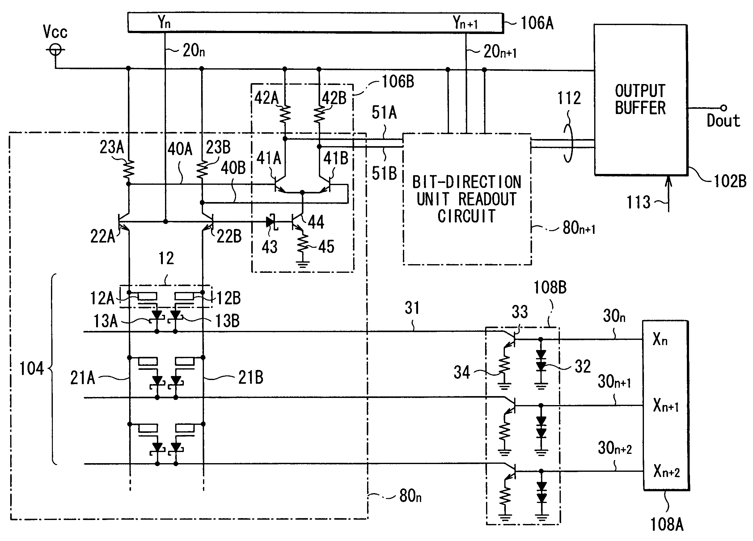
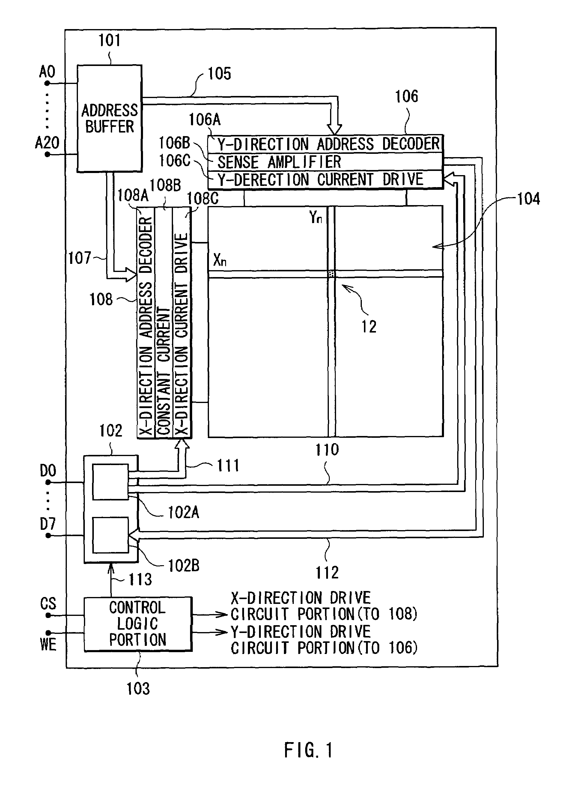
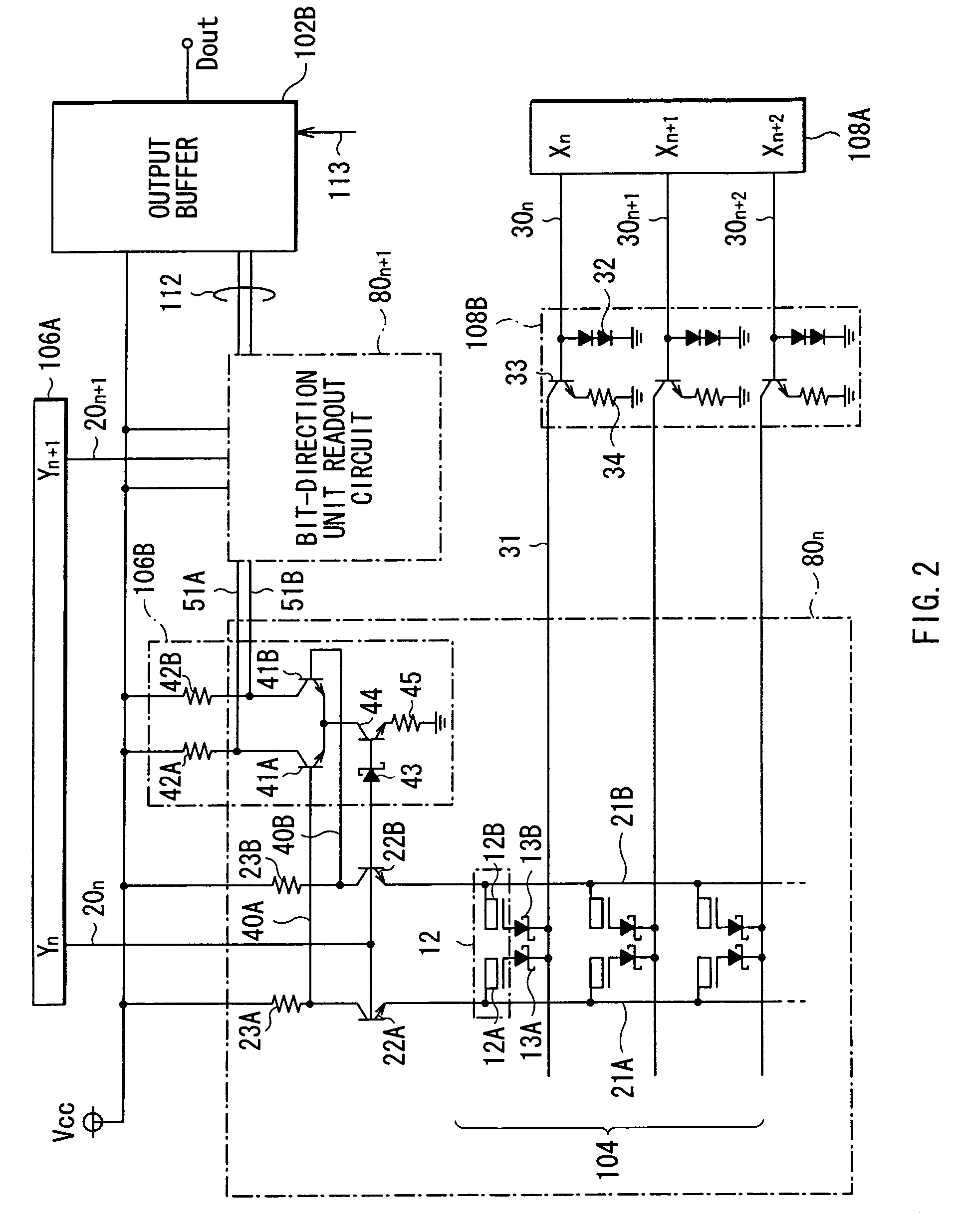
[0072]FIG. 1 is a diagram showing a general configuration of a magnetic memory device according to an embodiment of the invention. The magnetic memory device is an MRAM embodied as a so-called semiconductor memory chip and has, as main components, an address buffer 101, a data buffer 102, a control logic portion 103, a storage cell group 104, a Y-direction drive circuit portion 106, and an X-direction drive circuit portion 108. In the embodiment, the storage cell group 104 is disposed in a large area in the center of a silicon chip of the magnetic memory device, and circuit parts and wires such as the drive circuit portions 106 and 108 are mounted in a small area in the periphery.

[0073]The storage cell group 104 is obtained by disposing a number of storage cells 12 in a word line direction (X direction) and a bit line direction (Y direction) so as to form a matrix as a whole. Each of the storage cells 12 is the minimum unit of storing data. In each of the storage cells 12, bit data ...

second embodiment

[0191]A second embodiment of the present invention will now be described in detail with reference to FIGS. 25 to 32. The second embodiment has a characteristic different from that of the first embodiment in part of the configuration of the read circuit. In the following description, the same reference numerals are given to components which are substantially the same as those in the first embodiment and their description will not be repeated.

[0192]A magnetic memory device of the second embodiment has: the sense bit lines 21A and 21B as a read line pair extending in the bit line direction and supplying read current to the pair of magnetoresistive devices 12A and 12B; the sense word line 31 as an ground-side read line for leading the read current passed through the pair of magnetoresistive devices 12A and 12B to the ground; the constant current circuit 108B shared by the plurality of sense word lines 31 and specifying the sum of the pair of read currents flowing in the pair of magnetor...

modification 2-1

[0206]FIG. 26 shows a modification 2-1. In the modification, the diodes 13A and 13B shown in FIG. 25 are replaced with the bipolar transistors 63A and 63B. Further, in the modification, the bipolar transistors 63A and 64B function as a second semiconductor switch for selecting one of the plural storage cell groups 104X, and the read common line 85 for combining the plural sense word lines 31 of the storage cells 104Y to one is provided. The storage cell group 104Y is a concrete example of a “first-direction storage cell group” in the present invention.

[0207]In the circuit configuration of the magnetic memory device shown in FIG. 26, in reading operation, sensing current flows in a path described below.

[0208]In the case where the storage cell 12 in the Yn column and the Xn+1 row is selected as an object to be read, a selection signal is input to the Yn-th bit decode line 20n and the Xn+1-th word decode line 30n+1. The selection signal input to the bit decode line 20n is input to the ...


PUM


Abstract

The present invention provides a magnetic memory device capable of performing reading operation with lower power consumption and at high read precision and a method of reading the magnetic memory device. Sense bit lines (21A, 21B) are provided in a bit line direction for each pair of magnetoresistive devices (12A, 12B) constructing a storage cell (12) and a read current is supplied. The read currents passed through the pair of magnetoresistive devices (12A, 12B) flow to the ground via a sense word line (31). Further, by providing a constant current circuit (108B) commonly for plural sense word lines (31), the sum of a pair of read currents passing through the pair of magnetoresistive devices (12A, 12B) in one storage cell constant, and information is read from the storage cell (12) on the basis of the difference between the pair of read currents. By sharing the constant current circuit (108B), variations in the sum of the pair of read currents can be reduced, and power consumption can be also reduced.

Description

BACKGROUND OF THE INVENTION[0001]1. Field of the Invention[0002]The present invention relates to a magnetic memory device having a magnetoresistive device and a method of reading the same.[0003]2. Background Art[0004]Conventionally, as general memories used for an information processor such as a computer or a mobile communication device, volatile memories such as a DRAM (Dynamic Random Access Memory) and an SRAM (Static RAM) are used. If current is not always supplied to the volatile memories, all of information in the volatile memories is lost. Consequently, means for storing information, that is, a nonvolatile memory has to be provided, and a flash EEPROM, a hard disk device, or the like is used. In the nonvolatile memories, as the speed of information processing increases, increase in access speed is an important subject. Further, as a portable information device is being rapidly spread and its performance is becoming higher, development of an information device aiming at so-call...

Claims


Application Information

Patent Timeline
Patent Type & Authority Patents(United States)
IPC IPC(8): G11C11/00G11C11/15H01L21/8246H01L27/105H01L27/22H01L43/08
CPCB82Y10/00G11C11/15H01L27/228H01L27/226H01L27/224H10B61/20H10B61/10H10B61/22
Inventor EZAKI, JOICHIROKAKINUMA, YUJIKOGA, KEIJISUMITA, SHIGEKAZU
Owner TDK CORPARATION
Why Eureka
Try Eureka