Wafer level stack structure for system-in-package and method thereof

a stack structure and stack technology, applied in the field of electronic packaging technology, can solve the problems of no method of applying wlcsp to a sip, and the application of conventional sip b>10/b> is currently limited to the chip

Active Publication Date: 2007-05-08
SAMSUNG ELECTRONICS CO LTD
View PDF12 Cites 424 Cited by
  • Summary
  • Abstract
  • Description
  • Claims
  • Application Information

AI Technical Summary

Problems solved by technology

The conventional SIP 10 is currently limited to application at the chip level only.
Thus, there is currently no method of applying WLCSP to a SIP.

Method used


Image

  • Wafer level stack structure for system-in-package and method thereof
  • Wafer level stack structure for system-in-package and method thereof
  • Wafer level stack structure for system-in-package and method thereof

Examples


Embodiment Construction

[0027]Hereinafter, exemplary embodiments of the present invention will be described in detail with reference to the accompanying drawings.

[0028]In the Figures, the same reference numerals are used to denote corresponding elements throughout the Figures. It will be further appreciated that the figures are not drawn to scale. Rather, for simplicity and clarity of illustration, the dimensions of some of the elements are exaggerated relative to other elements.

[0029]In the description, well-known structures and processes have not been described or illustrated in detail to avoid obscuring the present invention. Further, the term “device-type” employed herein refers to one of a plurality of device types. For example, device types may include memory devices such as DRAM, SRAM, flash memory, or non-memory devices such as the CPU, ASIC, and other devices.

Chip Layout

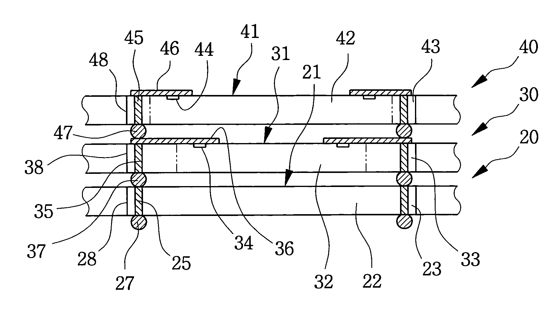
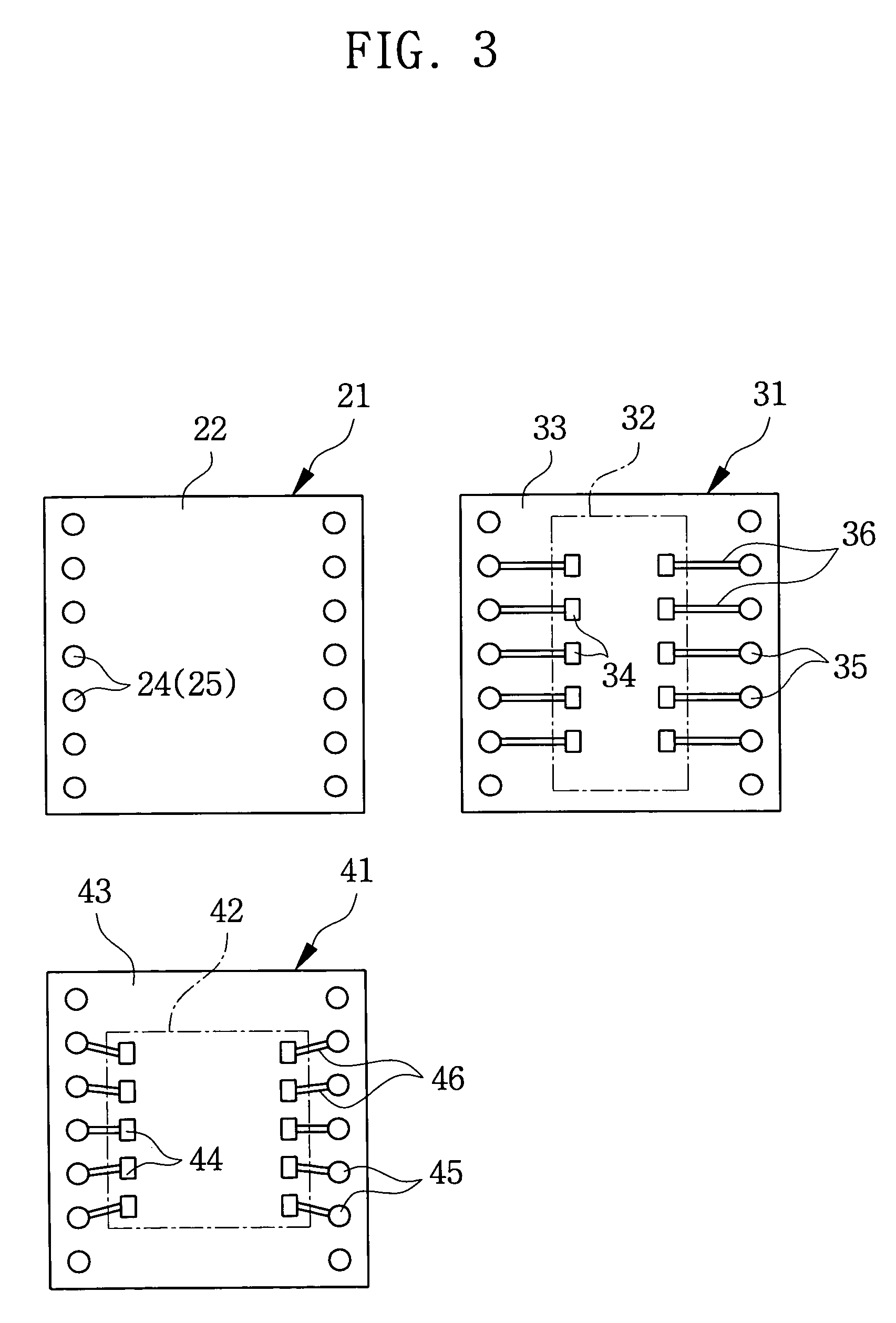
[0030]FIG. 3 illustrates a plan view of device chips of different device types according to an exemplary embodiment of the presen...


PUM


Abstract

A wafer level stack structure, including a first wafer including at least one first device chip of a first chip size, wherein each first device chip contains a first plurality of input / output (I / O) pads, a second wafer including at least one second device chip of a second chip size smaller than the first chip size, wherein each second device chip contains a second plurality of I / O pads, wherein the at least one second device chip is increased to the first chip size, wherein the first wafer and the second wafer are stacked, and wherein the first wafer and the second wafer are coupled to each other. A method of forming a wafer level stack structure, including forming a first wafer including at least one first device chip of a first chip size, wherein each first device chip contains a first plurality of input / output (I / O) pads, forming a second wafer including at least one second device chip of a second chip size smaller than the first chip size, wherein each second device chip contains a second plurality of I / O pads, wherein the at least one second device chip is increased to the first chip size, stacking the first wafer and the second wafer, and coupling the first wafer and the second wafer to each other. A system-in-package, including a wafer level stack structure including at least one first device chip with a first plurality of input / output (I / O) pads and at least one second device chip with a second plurality of I / O pads, and a common circuit board to which the wafer level stack structure is connected.

Description

CROSS REFERENCE TO RELATED APPLICATIONS[0001]This U.S. non-provisional application claims the benefit of priority under 35 U.S.C. §119 to Korean Patent Application No. 2003-82227 filed Nov. 19, 2003, the contents of which are incorporated herein in its entirety by reference.BACKGROUND OF THE INVENTION[0002]1. Field of the Invention[0003]The present invention relates to electronic packaging technology and more generally, to a wafer level stack structure in a system-in-package and method thereof.[0004]2. Description of the Related Art[0005]An electronic package, which may be referred to as a semiconductor package, may be defined as the housing and interconnection of integrated circuits, which may be referred to as the chip or the die, which may form an electronic system. The electronic package may include a structure to physically support the chip, a physical housing to protect the chip from the environment, a means of heat dissipation, and electrical connections to allow signal and p...

Claims


Application Information

Patent Timeline
Patent Type & Authority Patents(United States)
IPC IPC(8): H01L23/48H01L23/02H01L23/52H01L29/40H01L25/065
CPCH01L24/06H01L24/94H01L25/0657H01L25/50H01L23/481H01L24/05H01L23/3128H01L23/5389H01L24/16H01L2224/02372H01L2224/02379H01L2224/05009H01L2224/06181H01L2224/13025H01L2224/13099H01L2224/14181H01L2224/16145H01L2224/16227H01L2224/32014H01L2224/32145H01L2224/32225H01L2224/48095H01L2224/48227H01L2224/49171H01L2224/49175H01L2224/73265H01L2224/94H01L2225/06513H01L2225/06517H01L2225/06524H01L2225/06527H01L2225/06541H01L2225/06582H01L2225/06589H01L2924/014H01L2924/14H01L2924/1433H01L2924/15311H01L2924/30107H01L24/48H01L24/49H01L2924/01005H01L2924/01006H01L2924/01033H01L2224/16225H01L2224/0401H01L2224/04042H01L2924/00H01L2924/00014H01L2924/12042H01L2924/181H01L2224/16146H01L2924/00012H01L2224/45099H01L2224/45015H01L2924/207H01L23/48
Inventor LEE, KANG-WOOKOH, SE-YONGSONG, YOUNG-HEEKIM, GU-SUNG
Owner SAMSUNG ELECTRONICS CO LTD
Why Eureka
Try Eureka