Semiconductor chip with coil antenna and communication system

a technology of electromagnetic field and coil antenna, which is applied in the field of electromagnetic field, can solve the problems of difficult to obtain a larger electromotive force vtag than that required for driving a semiconductor chip, the data capacity is much larger than that of the magnetic card or bar code, and the reader cannot receive data accurately, etc., to achieve the effect of increasing the magnetic flux tag, high parasitic capacitance, and high inductan

Inactive Publication Date: 2008-04-08
HITACHI LTD
View PDF12 Cites 51 Cited by
  • Summary
  • Abstract
  • Description
  • Claims
  • Application Information

AI Technical Summary

Benefits of technology

[0019]In one aspect of the present invention for solving the above-mentioned problem there is provided a semiconductor chip having a coil antenna of a spiral figure and a circuit surface and provided with a communication unit for transmission and reception of signals to and from an external device by radio, the semiconductor chip having a construction for increasing the coupling efficiency between the antenna coil and the external device. The following modes can be considered as main examples of the construction for increasing the coupling coefficient between the antenna coil and the external device.

Problems solved by technology

Further, its data capacity is much larger than that of the magnetic card or bar code and is difficult to be influenced by stains or obstacles.
When a plurality of tags are present in an alternate magnetic field from the reader / writer, if the tags respond at random to a request command issued from the reader, signals will be superimposed on one another and the reader cannot receive data accurately.
In a small-sized coil antenna, the magnetic flux Φtag passing through a small loop area Stag is small and it is difficult to obtain a larger electromotive force Vtag than that required for driving a semiconductor chip.
The communication efficiency in a reply is also deteriorated.
However, in the former method, the working environment of RFID is greatly limited, and in the latter method, a reply from the chip is erased by a signal provided from the reader / writer and can no longer be read.
This has been a limitation on a mounting object of RFID, i.e., a group of applied products.

Method used


Image

  • Semiconductor chip with coil antenna and communication system
  • Semiconductor chip with coil antenna and communication system
  • Semiconductor chip with coil antenna and communication system

Examples


first embodiment

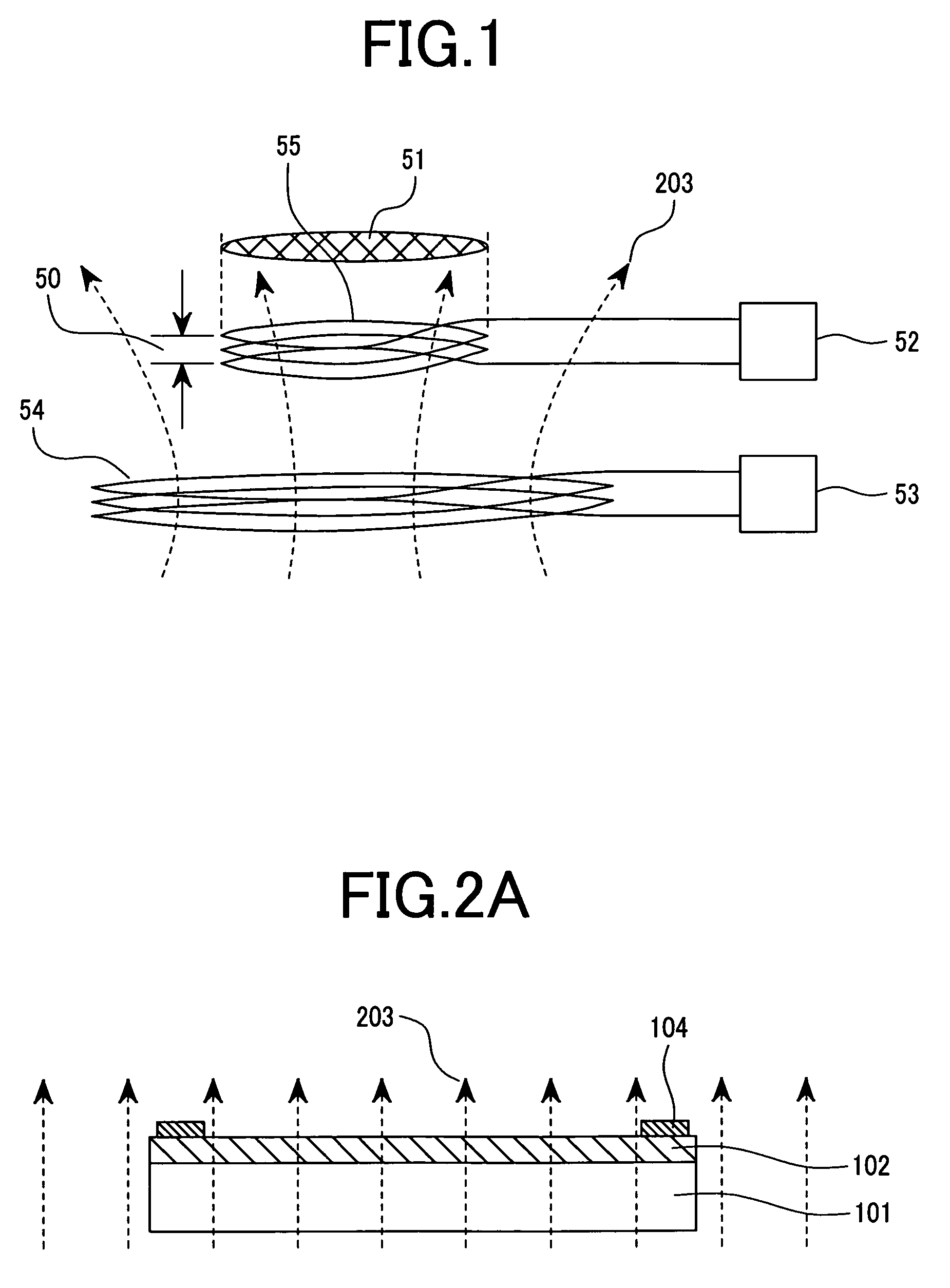
[0076]The construction of a semiconductor chip having a sensor function according to a first embodiment is shown schematically in FIG. 5. A reader / writer 201 is disposed with respect to the semiconductor chip indicated at 100. The reader / writer 201 has the function of transmitting an alternate magnetic field to the semiconductor chip 100 having a sensor function and receiving a reply from the same chip. The reader / writer 201 is controlled by a controller 200 such as a PC (Personal Computer). A spiral transformer 206 or the like is used in the transmitter of the reader / writer 201.

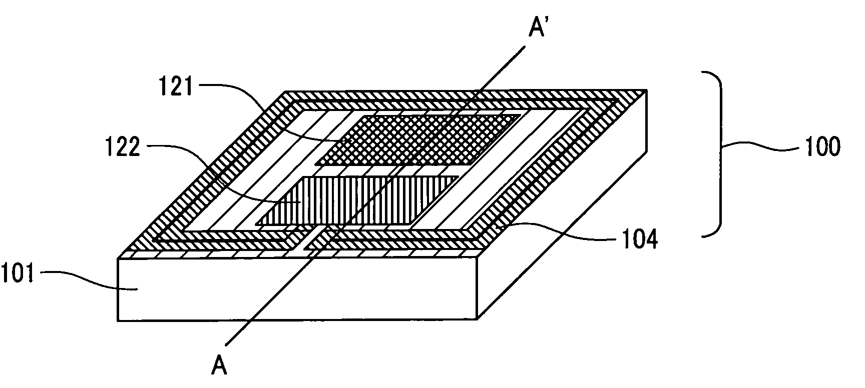
[0077]On the other hand, the semiconductor chip 100 having a sensor function is in the form of an individual chip obtained by dicing and an internal configuration thereof, when classified according to functions, can be divided into an antenna section 207, an RF section 208, a control section 209, and a sensor section 210. The antenna section 207 is adapted to receive an alternate magnetic field 203 necessary...

second embodiment

[0096]In a second embodiment, a semiconductor chip 99 uses its ID information as an object of radio communication. That is, the semiconductor chip 99 does not have a sensor function. For the purpose of enhancing the electromagnetic coupling of the chip, the semiconductor chip 99 is configured such that a magnetic material is disposed in a hole formed by half etching in a silicon substrate on the back side of an integrated circuit.

[0097]The configuration of the semiconductor chip 99 of this embodiment is shown schematically in FIG. 12. A reader / writer 201 is controlled by a controller 200 such as PC and has a function of transmitting an electromagnetic field to the semiconductor chip 99 and receiving a reply from the same chip. This transmitter section is composed of a transformer 206 of a spiral figure. On the other hand, an internal configuration of the semiconductor chip 99 can be divided according to functions into an antenna section 207, an RF section 208, and a control section ...

third embodiment

[0106]In a third embodiment, a magnetic material is disposed in accordance with another structure in the semiconductor chip 100 of the first embodiment. In all of the following examples it is preferable that a dicing process into individual chips be carried out after the formation of a magnetic material.

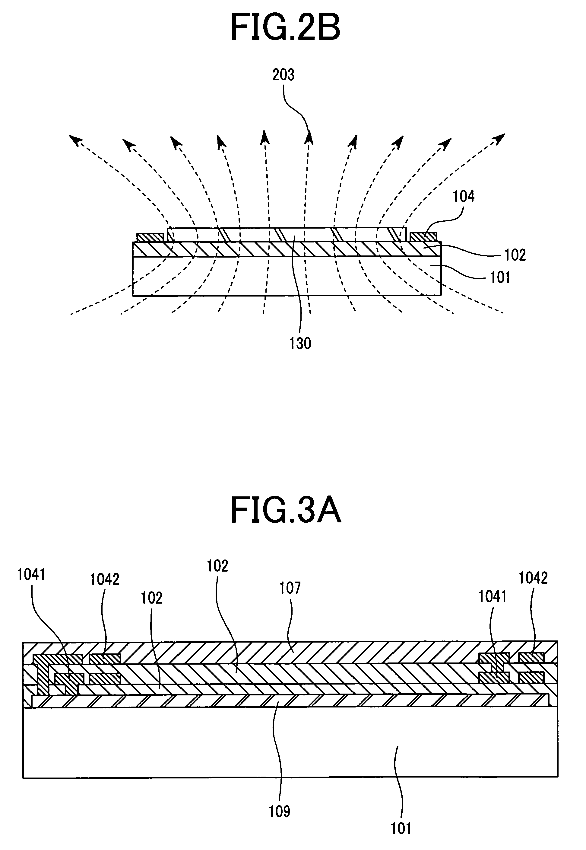
[0107]FIG. 15 is a cross-sectional view showing an example in which a magnetic material 130 is bonded inside the coil antenna 104. After the coil antenna 104 is formed in the same way as in the first embodiment, the magnetic material 130 is formed by bonding so as not to overlap the ion sensitive FET 122 and the reference electrode 130. The number of processes required for affixing the sensitive material 130 is small and hence it is possible to effect a less expensive manufacture.

[0108]FIG. 16 is a cross-sectional view showing an example in which a resin with a magnetic material 131 dispersed therein as the protective polyimide 107 is stacked and bonded.

[0109]In the semiconductor chi...


PUM

PropertyMeasurementUnit
resonance frequenciesaaaaaaaaaa
resonance frequencyaaaaaaaaaa

Abstract

The present invention intends to prevent the communication distance from becoming shorter with a reduction in size of a coil antenna to the chip size and with a consequent decrease of an induced voltage. According to the present invention there is provided a semiconductor chip having a coil antenna and a circuit surface and adapted to transmit and receive signals by radio to and from an external device. The semiconductor chip has a configuration for increasing an electromagnetic coupling coefficient between the coil antenna and the external device. According to a concrete example thereof, a magnetic material is disposed, the coil antenna is formed by a stacked structure comprising plural conductor layers and insulating layers superimposed one on another, or the coil antenna is disposed outside an external form of a circuit of the semiconductor chip.

Description

CLAIM OF PRIORITY[0001]The present application claims priority from Japanese application JP 2004-033293 filed on Feb. 10, 2004, the content of which is hereby incorporated by reference into this application.[0002]1. Field of the Invention[0003]The present invention relates to a semiconductor chip for transmission and reception of signals by radio to and from an external device, and more particularly, to a semiconductor chip having a configuration for increasing a coupling coefficient between a coil antenna and an external device, and a communication system using the semiconductor chip.[0004]2. Related Art[0005]RFID (Radio Frequency Identification) wherein a radio signal is provided from an external device (reader / writer) and information stored in memory in a tag is read, is now being noted as a basic technique for the ubiquitous society. Radio communication techniques using 13.56 MHz and 2.45 GHz defined by the radio law as resonance frequencies have been developed in Japan.[0006]An...

Claims


Application Information

Patent Timeline
Patent Type & Authority Patents(United States)
IPC IPC(8): H01L23/02G06K19/077G06K19/07H01F17/04H01L21/822H01L23/48H01L23/522H01L23/538H01L27/04H01Q1/22H01Q7/00H01Q7/06
CPCG06K7/10178G06K19/07749G06K19/07756G06K19/07775G06K19/07779G06K19/07783G06K19/07784H01L23/48H01L23/5227H01Q1/22H01Q1/2225H01Q7/00H01L2924/0002H01L2924/3011H01L2924/00H01L2223/6677H01L2224/04105
Inventor HASEBE, TAKEHIKOGOTO, YASUSHIUESAKA, KOUICHIYAZAWA, YOSHIAKITORIGOE, MAKOTO
Owner HITACHI LTD
Why Eureka
Try Eureka