Semiconductor Metrology Based On Hyperspectral Imaging

a technology of hyperspectral imaging and metrology, applied in semiconductor/solid-state device testing/measurement, optical radiation measurement, instruments, etc., can solve the problem of limited number of locations that can be measured for a given wafer throughput requirement, time-consuming model-based metrology techniques, and insufficient signal information for typical imaging-based measurements to directly measure complex three-dimensional structures that are commonly manufactured today. problem, to achieve the effect of improving coupling efficiency

Active Publication Date: 2020-07-16
KLA TENCOR TECH CORP
View PDF0 Cites 5 Cited by
  • Summary
  • Abstract
  • Description
  • Claims
  • Application Information

AI Technical Summary

Benefits of technology

[0013]In another further aspect, a fiber array collector includes a corresponding array of micro-lenses or micro-mirrors configured to control beam divergence and improve coupling efficiency. Each micro-lens of the array couples light into or out of an individual fiber optical element.

Problems solved by technology

Although non-imaging, model-based optical metrology techniques offer high precision measurement capability, the number of locations that can be measured for a given wafer throughput requirement is limited.
The measurement of dedicated metrology structures by traditional non-imaging, model-based metrology techniques is time consuming.
Unfortunately, typical imaging-based measurements lack sufficient signal information to directly measure complex three dimensional structures that are commonly manufactured today.
For this reason, traditional image based metrology algorithms cannot perform reliably with arbitrary targets or device structures.
Future metrology applications present challenges for image based metrology due to increasingly small resolution requirements and the increasingly high value of wafer area.

Method used


Image

  • Semiconductor Metrology Based On Hyperspectral Imaging
  • Semiconductor Metrology Based On Hyperspectral Imaging
  • Semiconductor Metrology Based On Hyperspectral Imaging

Examples


embodiment 150

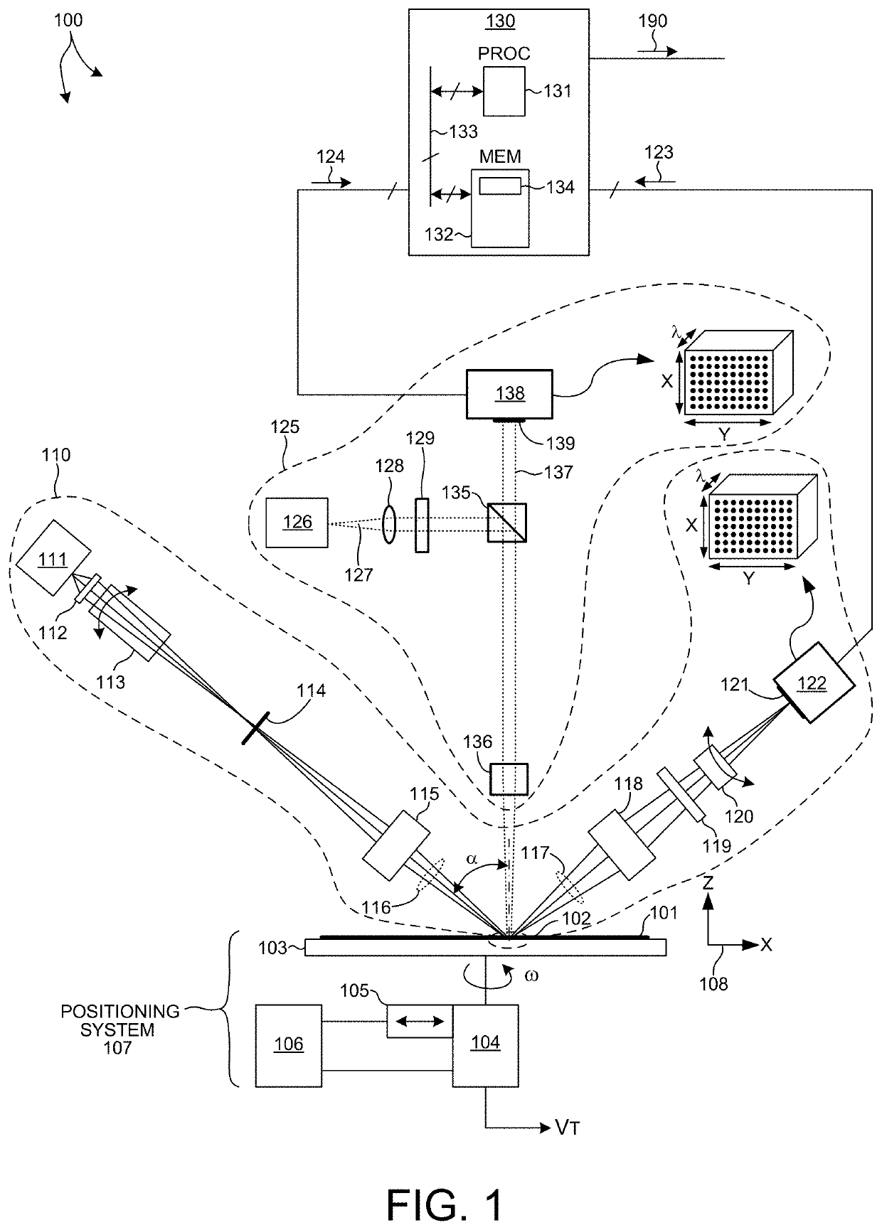
[0088]FIG. 7 depicts an embodiment 150 of a combined fiber optics illuminator / collector including an array of micro-lenses 151. In the embodiment depicted in FIG. 7, each fiber is employed as an illuminator and a collector. Furthermore, as depicted in FIG. 7, each micro-lens of the array of micro-lenses 151 is configured to collimate illumination light provided to specimen 101.

embodiment 152

[0089]FIG. 8 depicts an embodiment 152 of a combined fiber optics illuminator / collector including an array of micro-lenses153. In the embodiment depicted in FIG. 8, each fiber is employed as an illuminator and a collector. Furthermore, as depicted in FIG. 8, each micro-lens of the array of micro-lenses 153 is configured to focus illumination light provided to specimen 101.

[0090]FIG. 9 depicts a fiber optics illuminator 154 including a plurality of illumination fiber optical elements and a fiber optics collector 155 including a plurality of collection fiber optical elements. The configuration depicted in FIG. 9 is suitable for oblique incidence measurements. As depicted in FIG. 9, an array of micro-lenses 156 focuses illumination light provided to specimen 101, and an array of micro-lenses 157 collects light from specimen 101 in response to the illumination light. In another embodiment (not shown), the array of micro-lenses 156 is configured to collimate illumination light provided t...


PUM

PropertyMeasurementUnit
wavelengthsaaaaaaaaaa
wavelengthaaaaaaaaaa

Abstract

Methods and systems for performing semiconductor measurements based on hyperspectral imaging are presented herein. A hyperspectral imaging system images a wafer over a large field of view with high pixel density over a broad range of wavelengths. Image signals collected from a measurement area are detected at a number of pixels. The detected image signals from each pixel are spectrally analyzed separately. In some embodiments, the illumination and collection optics of a hyperspectral imaging system include fiber optical elements to direct illumination light from the illumination source to the measurement area on the surface of the specimen under measurement and fiber optical elements to image the measurement area. In another aspect, a fiber optics collector includes an image pixel mapper that couples a two dimensional array of collection fiber optical elements into a one dimensional array of pixels at the spectrometer and the hyperspectral detector.

Description

TECHNICAL FIELD[0001]The described embodiments relate to metrology systems and methods, and more particularly to methods and systems for improved measurement of semiconductor structures.BACKGROUND INFORMATION[0002]Semiconductor devices such as logic and memory devices are typically fabricated by a sequence of processing steps applied to a specimen. The various features and multiple structural levels of the semiconductor devices are formed by these processing steps. For example, lithography among others is one semiconductor fabrication process that involves generating a pattern on a semiconductor wafer. Additional examples of semiconductor fabrication processes include, but are not limited to, chemical-mechanical polishing, etch, deposition, and ion implantation. Multiple semiconductor devices may be fabricated on a single semiconductor wafer and then separated into individual semiconductor devices.[0003]Metrology processes are used at various steps during a semiconductor manufacturi...

Claims


Application Information

Patent Timeline
Patent Type & Authority Applications(United States)
IPC IPC(8): G01N21/3563G01J3/28H01L21/66G01N21/21
CPCG01N21/3563G01N2021/3568G01N21/211H01L22/12G01J3/2823G01N2021/213G01N2201/08G01N21/9501H01L22/20G01J3/0208G01J3/0218
Inventor WANG, DAVID Y.BUETTNER, ALEXANDERPANDEV, STILIAN IVANOVSAERCHEN, EMANUELSHCHEGROV, ANDREI V.BLASENHEIM, BARRY
Owner KLA TENCOR TECH CORP
Why Eureka
Try Eureka