
High-Frequency Vacuum Electronic Device

a vacuum electronic device and high-frequency technology, applied in the direction of transit-tube cathodes, transit-tube circuit elements, traveling-wave tubes, etc., can solve the problem of elusive power levels of compact and robust devices producing terahertz radiation in meaningful power levels (milliwatts or higher), and achieve the effect of improving coupling efficiency

Active Publication Date: 2019-09-12
WISCONSIN ALUMNI RES FOUND +1
View PDF0 Cites 6 Cited by
  • Summary
  • Abstract
  • Description
  • Claims
  • Application Information

AI Technical Summary

Benefits of technology

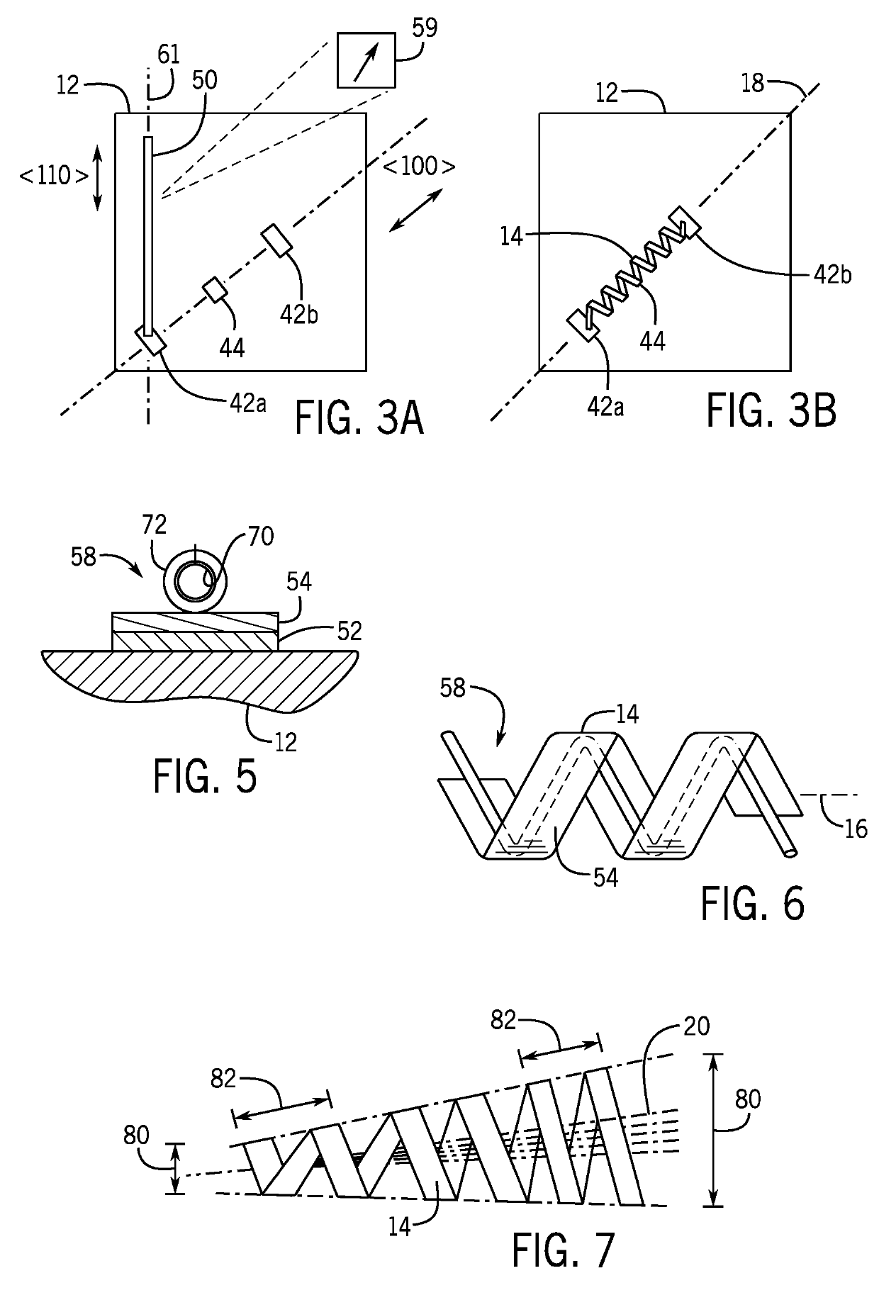
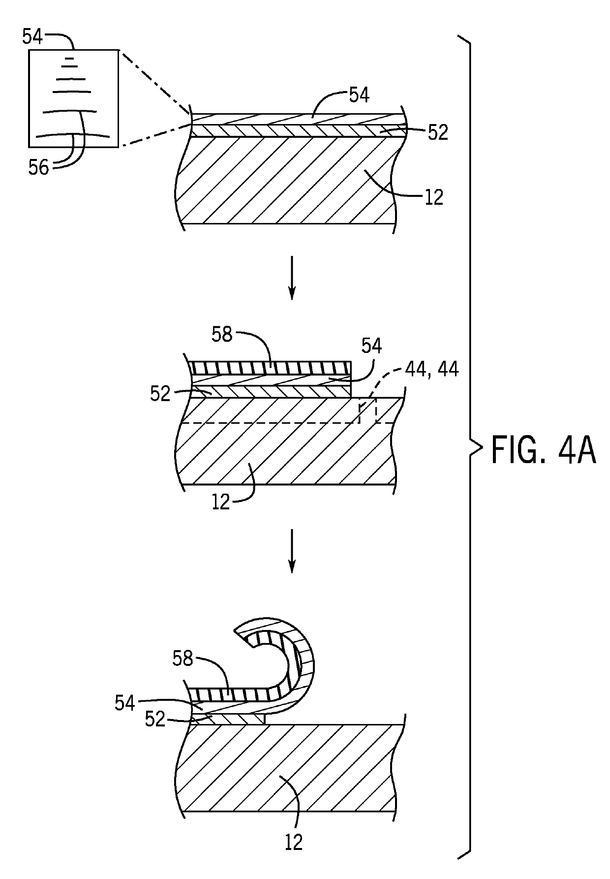
The invention provides small-scale helices that can be used in structures like traveling-wave tubes. These helices are formed through a self-assembly process that releases stress. The invention also includes a mechanism that allows for slowing down of the electron beam as it releases energy. This slowing produces a parallel slowing of the electromagnetic wave, which improves coupling efficiency.

Problems solved by technology

The production and amplification of terahertz electromagnetic radiation may prove important in a variety of technologies including imaging, spectroscopy, and data communication; however, the ability to produce compact and robust devices producing terahertz radiation in meaningful power levels (milliwatts or higher) is elusive.
A challenge in producing a traveling-wave tube in the terahertz range is the small size of the helix required for these frequencies that must be precisely fabricated and aligned with an electron beam.

Method used


Image

  • High-Frequency Vacuum Electronic Device
  • High-Frequency Vacuum Electronic Device
  • High-Frequency Vacuum Electronic Device

Examples


Embodiment Construction

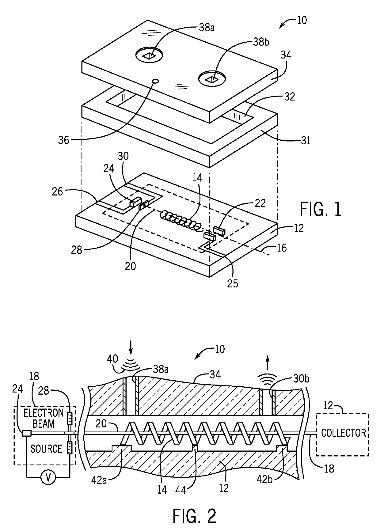
[0051]Referring now to FIGS. 1 and 2, a vacuum electronic device 10 in an embodiment of the traveling-wave tube may be constructed on a planar substrate 12 using standard integrated circuit techniques. The planar substrate 12 may support a helical conductor 14 extending along an axis 16 coplanar with the upper surface of the substrate 12 fabricated on that substrate as will be described below.

[0052]Disposed at a first end of the helical conductor 14 along axis 16 is an electron beam source 18 directing an electron beam 20 along the axis 16 concentrically within the helical conductor 14. The opposite end of the helical conductor 14 provides electron collector 22, collecting and dissipating residual energy in the electron beam 20 after passing through the helical conductor 14.

[0053]The electron beam source 18 may provide a cathode 24 connected to a source of negative voltage through conductive trace 26 and operates to emit electrons (for example, by field emission) accelerated through...


PUM


Abstract

A self-assembling element fabricated using integrated circuit techniques may provide a small diameter helical conductor surrounding an electron beam for the construction of a vacuum electronic device such as a traveling-wave tube for terahertz scale signal.

Description

STATEMENT REGARDING FEDERALLY SPONSORED RESEARCH OR DEVELOPMENT[0001]This invention was made with government support under DE-FG02-03ER46028 awarded by the US Department of Energy. The government has certain rights in the invention.CROSS REFERENCE TO RELATED APPLICATIONBACKGROUND OF THE INVENTION[0002]The present invention relates to vacuum electronic devices employing an interacting electron beam and electromagnetic wave (such as in a traveling-wave tube) and in particular such devices providing extremely high-frequency operation.[0003]Terahertz electromagnetic waves have a frequency that lies between microwaves and infrared light. The production and amplification of terahertz electromagnetic radiation may prove important in a variety of technologies including imaging, spectroscopy, and data communication; however, the ability to produce compact and robust devices producing terahertz radiation in meaningful power levels (milliwatts or higher) is elusive.[0004]One potential candidat...

Claims


Application Information

Patent Timeline
Patent Type & Authority Applications(United States)
IPC IPC(8): H01J25/02
CPCH01J25/02H01J9/14H01J9/24H01J23/04H01J23/26H01J25/36
Inventor VAN DER WEIDE, DANIEL W.LAGALLY, MAXCAVALLO, FRANCESCA
Owner WISCONSIN ALUMNI RES FOUND
Learn More