Method of fabricating non-volatile memory device

a memory device and non-volatile technology, applied in the field of memory, can solve the problems of continuously reducing the size of the device and reducing the stored capacitance of the memory device accordingly, and achieve the effect of improving the coupling efficiency of the memory device and simple and cheap processes

Inactive Publication Date: 2012-10-18
MAXCHIP ELECTRONICS CORP
View PDF5 Cites 4 Cited by
  • Summary
  • Abstract
  • Description
  • Claims
  • Application Information

AI Technical Summary

Benefits of technology

[0008]The invention is directed to a method of fabricating a non-volatile memory device capable of increasing the coupled area between the floating gate and the control gate to improve the coupling efficiency of the memory device by simple and cheap processes.
[0021]In the invention, the uneven surface is formed to increase the coupled area between the floating gate and the control gate. Thereby, the coupling efficiency of the memory device is improved and the layout area is reduced under the same coupled area. In addition, the trenches are formed simultaneously with the formation of the isolation structures, and no additional mask is needed. Accordingly, the fabricating method of the invention is simple and the cost thereof is cheap.

Problems solved by technology

However, with the demand of the minimization of the devices, the size of the devices is continuously diminished, and the stored capacitance in the memory device is reduced accordingly.

Method used


Image

  • Method of fabricating non-volatile memory device
  • Method of fabricating non-volatile memory device
  • Method of fabricating non-volatile memory device

Examples


Embodiment Construction

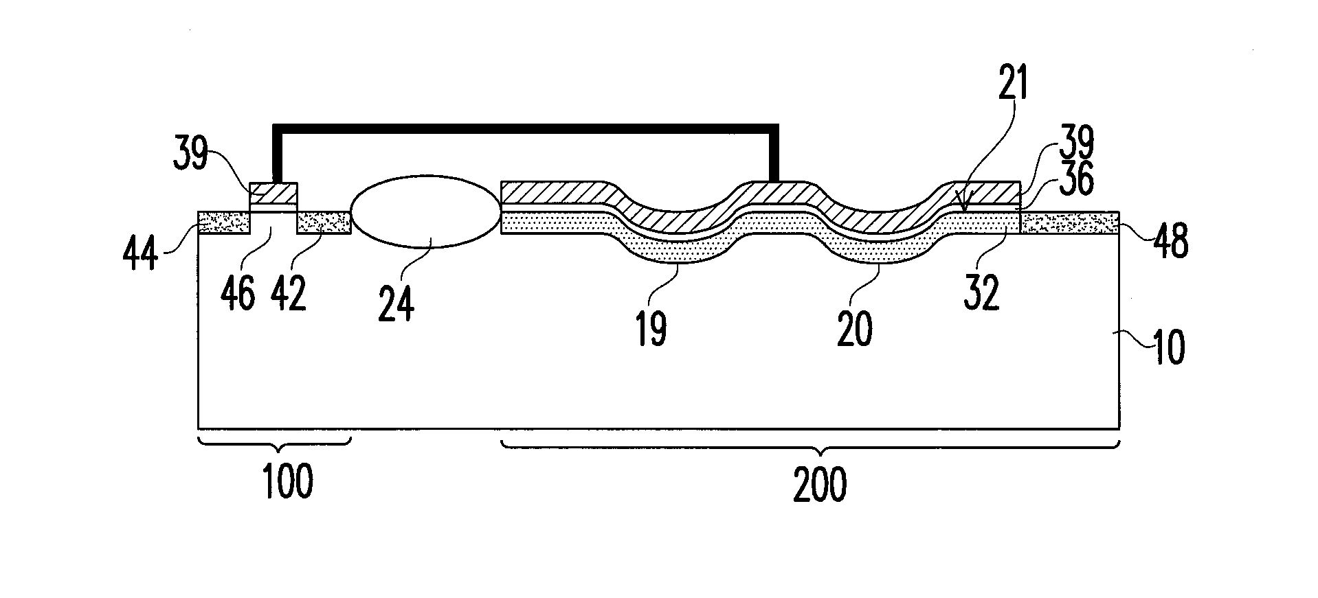
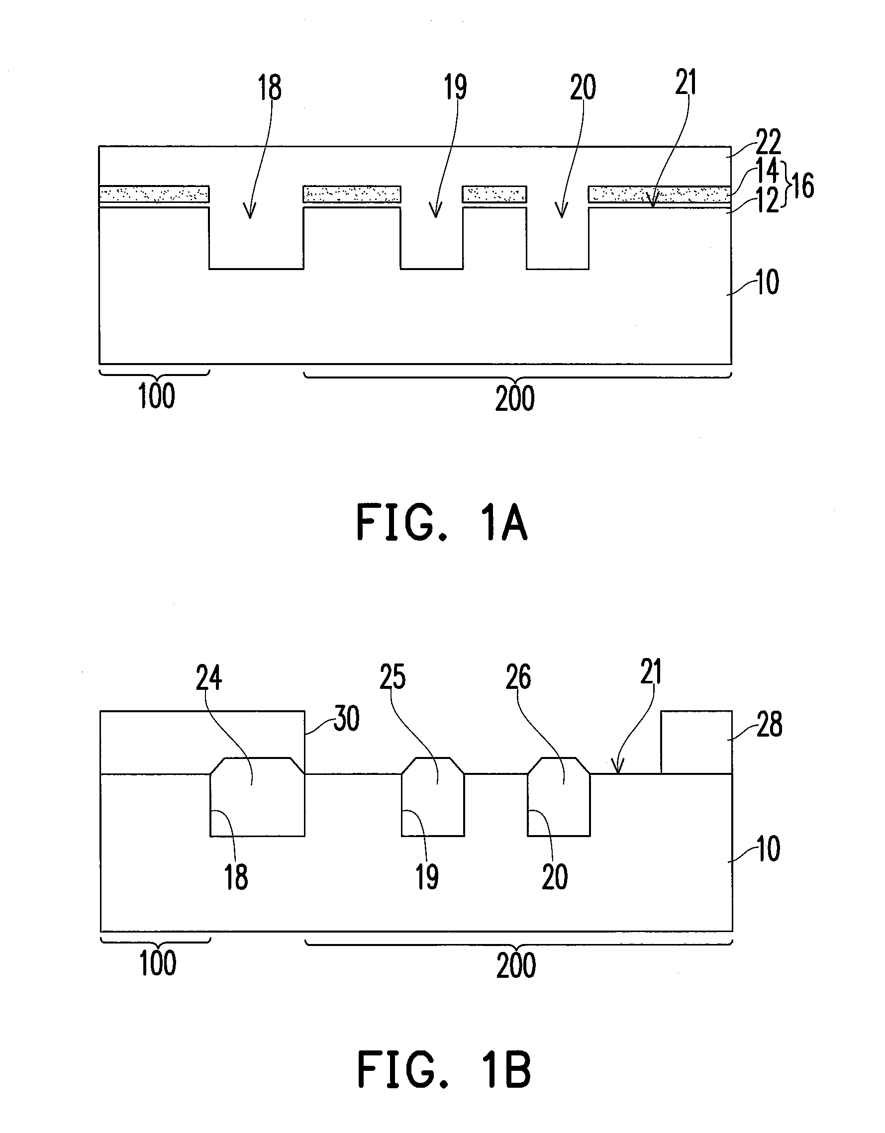
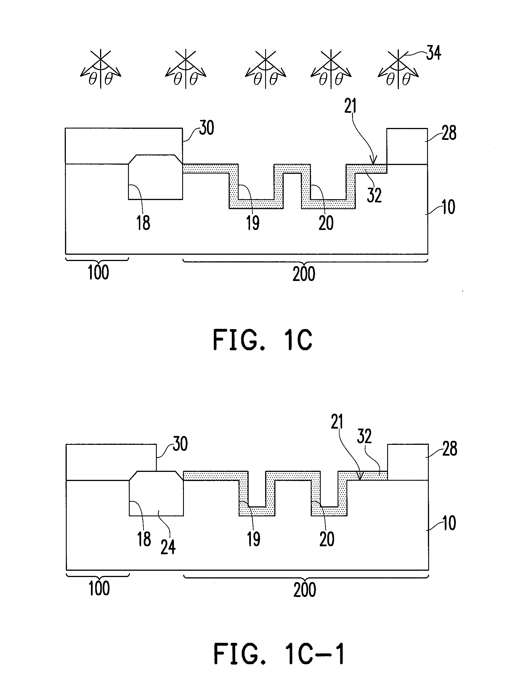
[0026]FIG. 1E is a schematic cross-sectional view of a non-volatile memory device according to one embodiment of the present invention. FIG. 2E is a schematic cross-sectional view of a non-volatile memory device according to another embodiment of the present invention.

[0027]Referring to FIGS. 1E and 2E, a non-volatile memory device of an embodiment of the invention includes a substrate 10, a dielectric layer 36, a floating gate 39, source and drain regions 42 and 44, a channel region 46, and a doped layer 32. The substrate 10 is, for example, a bulk substrate such as a silicon substrate or a silicon-on-insulator (SOI) substrate. The substrate 10 includes a first region 100 and a second region 200. The first region 100 is separated from the second region 200 by an isolation structure 24. The isolation structure 24 is, for example, a shallow trench isolation structure or a field oxide layer. The substrate 10 has a flat surface in the first region 100, and the substrate 10 has a plural...


PUM


Abstract

A method of fabricating a non-volatile memory device is provided. A substrate including a first region and a second region is provided. Then, an uneven surface is formed on the substrate in the second region. Thereafter, a doped layer is formed in the substrate in the second region, and the doped layer is served as a control gate. Afterward, a dielectric layer is formed on the substrate in the first region and on the uneven surface of the substrate in the second region. Next, a floating gate is formed on the dielectric layer, and the floating gate is extended from the first region to the second region. Source and drain regions are formed in the substrate at opposite sides of the floating gate in the first region.

Description

CROSS-REFERENCE TO RELATED APPLICATION[0001]This application is a Divisional of and claims the priority benefit of U.S. patent application Ser. No. 12 / 635,703, filed on Dec. 11, 2009, now pending, which claims the priority benefits of Taiwan application Serial No. 98135654, filed on Oct. 21, 2009. The entirety of each of the above-mentioned patent applications is hereby incorporated by reference herein and made a part of this specification.BACKGROUND OF THE INVENTION[0002]1. Field of the Invention[0003]The invention relates to a memory and method of fabricating the same, and more particularly, to a non-volatile memory and a method of fabricating the same.[0004]2. Description of Related Art[0005]The non-volatile memory device has the advantages of executing data write, read and erase for many times, and the stored data will not disappear while the power is off. Therefore, the non-volatile memory device is commonly applied in the electronic products.[0006]A typical non-volatile memory...

Claims


Application Information

Patent Timeline
Patent Type & Authority Applications(United States)
IPC IPC(8): H01L21/336
CPCH01L27/1203H01L29/7881H01L29/42324
Inventor CHEN, CHUNG-YICHEN, LI-YEATLIN, JUNG-CHUN
Owner MAXCHIP ELECTRONICS CORP
Why Eureka
Try Eureka