

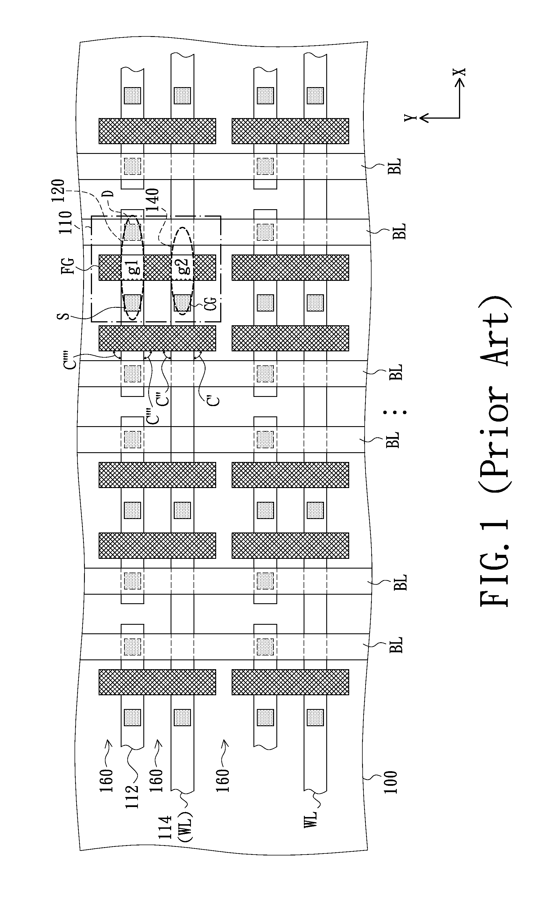
Non-Volatile Memory Cell and Layout Structure of Non-Volatile Memory Device
a non-volatile memory and layout structure technology, applied in the direction of semiconductor devices, electrical devices, transistors, etc., can solve the problems of high cost, poor device yield, and complicated manufacturing process of embedded memory devices using double-poly non-volatile memory devices, so as to reduce the leakage current produced at the corners of isolation structures, reduce the coupling efficiency, and reduce the effect of corners
- Summary
- Abstract
- Description
- Claims
- Application Information
AI Technical Summary
Benefits of technology
Problems solved by technology
Method used
Image

Examples
Embodiment Construction
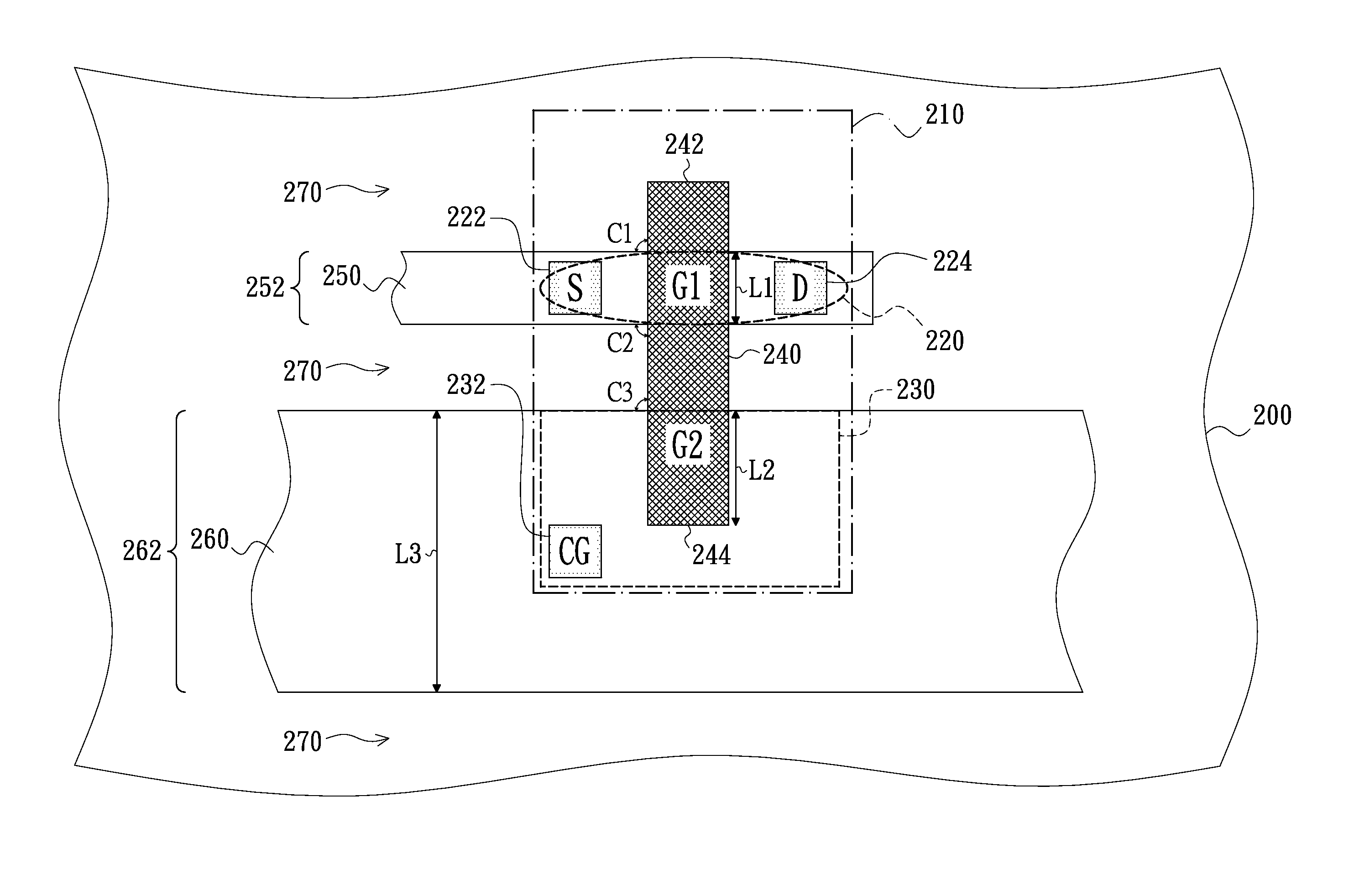
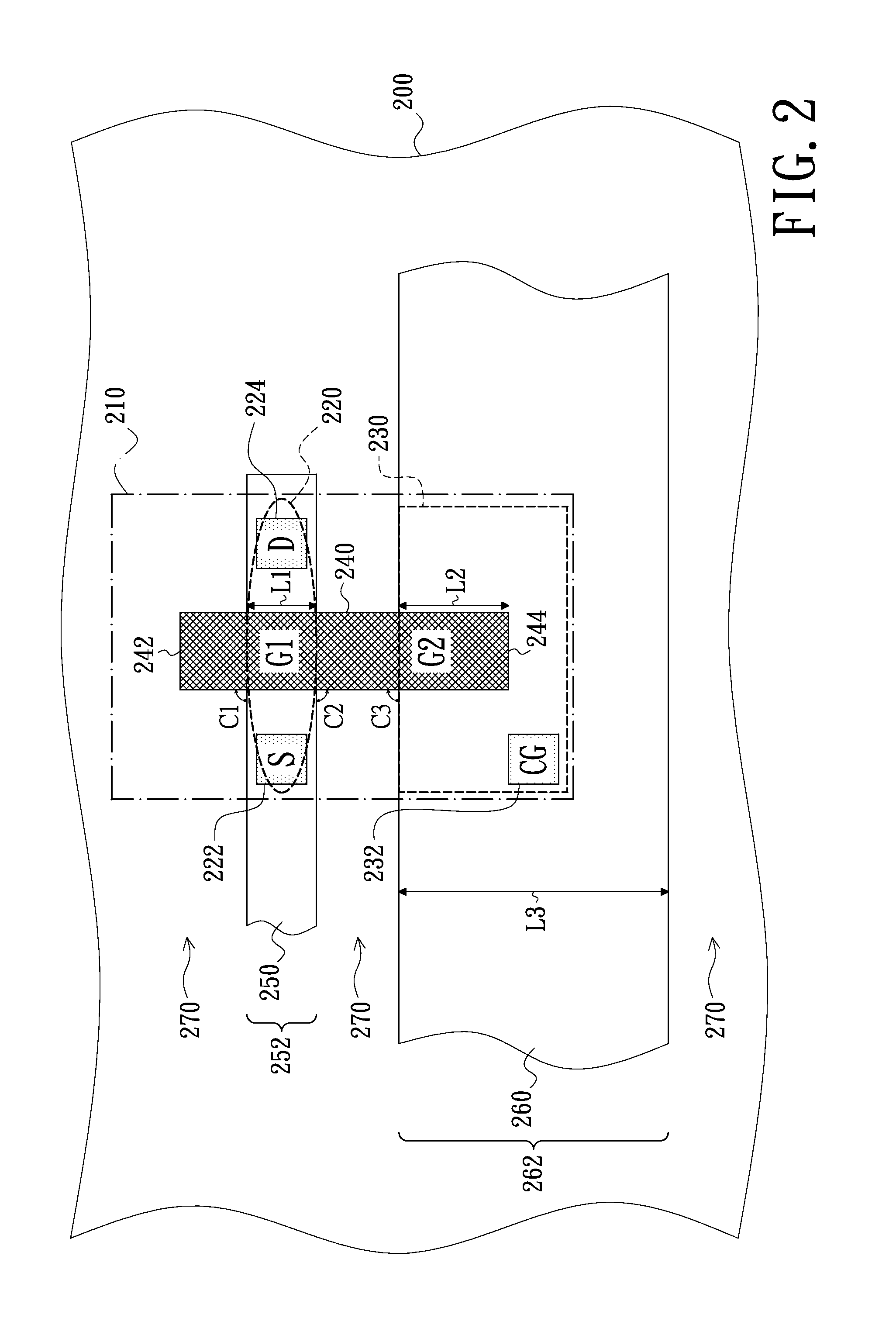
[0035]FIG. 2 is a schematic top view of a non-volatile memory cell in accordance with an embodiment of the present invention.
[0036]As illustrated in FIG. 2, the non-volatile memory cell 210 is comprised of a semiconductor substrate 200, a conductor 240, a plurality of isolation structures 270, a first-type doped well 260, two first ion doped regions 222, 224 and a second ion doped region 232.
[0037]The semiconductor substrate 200 has the isolation structures 270 arranged in parallel with one another and disposed therein. The isolation structures 270 are for example shallow trench isolation (STI) structures. The isolation structures 270 define a transistor region 252 and a capacitor region 262 in parallel with the transistor region 252 in the semiconductor substrate 200. The first-type doped well 260 is disposed in the capacitor region 262 and is for example an N-type doped well.
[0038]In the illustrated embodiment, the semiconductor substrate 200 is for example a non-doped semiconduct...
PUM
 Abstract
Description
Claims
Application Information