Apparatus and methods related to ground paths implemented with surface mount devices

a surface mount device and ground path technology, applied in the direction of manufacturing tools, semiconductor/solid-state device details, printed circuit non-printed electric components association, etc., can solve problems such as degrading the performance of wireless devices

Active Publication Date: 2014-10-16
SKYWORKS SOLUTIONS INC
View PDF30 Cites 51 Cited by
  • Summary
  • Abstract
  • Description
  • Claims
  • Application Information

AI Technical Summary

Benefits of technology

[0007]In some embodiments, the RF module can further include a conductive racetrack implemented under the plurality of shielding-wirebonds. The conductive racetrack can be electrically connected to the shielding-wirebonds and a ground plane within the packaging substrate. The RF shield can include the at least one shielding-component positioned along a selected edge of the packaging substrate. The selected edge can be substantially free of shielding-wirebond and conductive racetrack. The selected edge can be substantially free of a margin for accommodating the shielding-wirebond and the conductive racetrack, thereby reducing the overall lateral area of the packaging substrate.
[0011]In some embodiments, forming of the RF shield includes mounting the at least one shielding-component positioned along a selected edge of the packaging substrate. The selected edge can be substantially free of shielding-wirebond. The selected edge can be substantially free of a margin for accommodating the shielding-wirebond, thereby reducing the overall lateral area of the packaging substrate.
[0013]In accordance with some implementations, the present disclosure relates to a radio-frequency (RF) module that includes a packaging substrate configured to receive a plurality of components and including a ground plane. The RF module further includes a conductive layer implemented over the packaging substrate. The RF module further includes a surface mount device (SMD) mounted on the packaging substrate. The SMD is configured to electrically connect the conductive layer with the ground plane to thereby provide RF shielding between first and second regions about the SMD.
[0017]In a number of implementations, the present disclosure relates to a method for fabricating a radio-frequency (RF) module. The method includes providing a packaging substrate, where the packaging substrate is configured to receive a plurality of components and includes a ground plane. The method further includes mounting a surface mount device (SMD) on the packaging substrate. The method further includes forming or providing a conductive layer over the SMD such that the SMD electrically connects the conductive layer with the ground plane to thereby provide RF shielding between first and second regions about the SMD.
[0019]According to some implementations, the present disclosure relates to a wireless device that includes an antenna and a module in communication with the antenna. The module is configured to facilitate processing of an RF signal through the antenna. The module includes a packaging substrate configured to receive a plurality of components and having a ground plane. The module further includes a conductive layer implemented over the packaging substrate. The module further includes a surface mount device (SMD) mounted on the packaging substrate. The SMD is configured to electrically connect the conductive layer with the ground plane to thereby provide RF shielding between first and second regions about the SMD.

Problems solved by technology

Electromagnetic (EM) fields can be generated from or have an undesirable effect on a region of a radio-frequency (RF) device such as an RF module.
Such an EM interference (EMI) can degrade the performance of wireless devices that use such an RF module.

Method used


Image

  • Apparatus and methods related to ground paths implemented with surface mount devices
  • Apparatus and methods related to ground paths implemented with surface mount devices
  • Apparatus and methods related to ground paths implemented with surface mount devices

Examples


Embodiment Construction

[0057]The headings provided herein, if any, are for convenience only and do not necessarily affect the scope or meaning of the claimed invention.

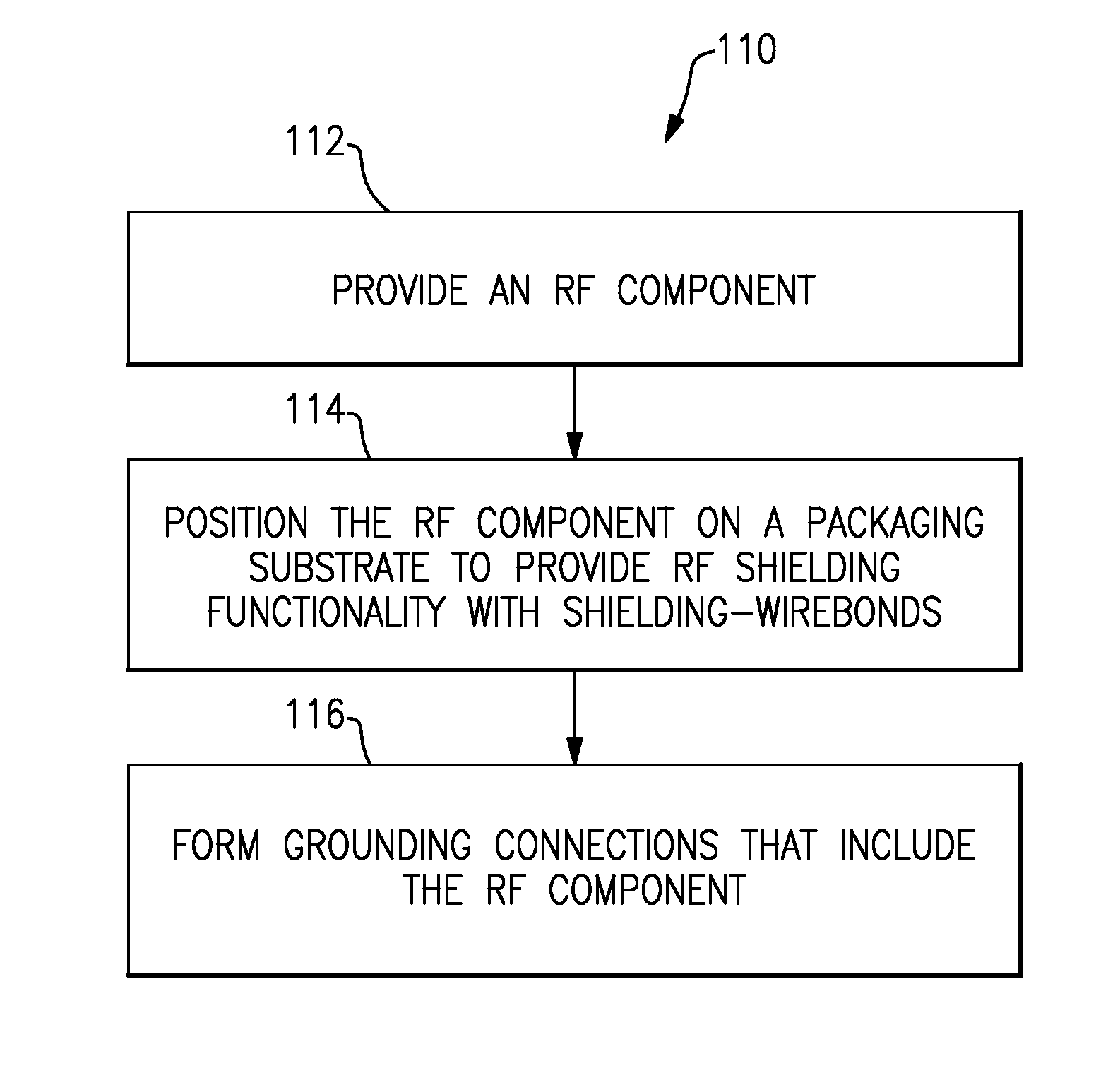
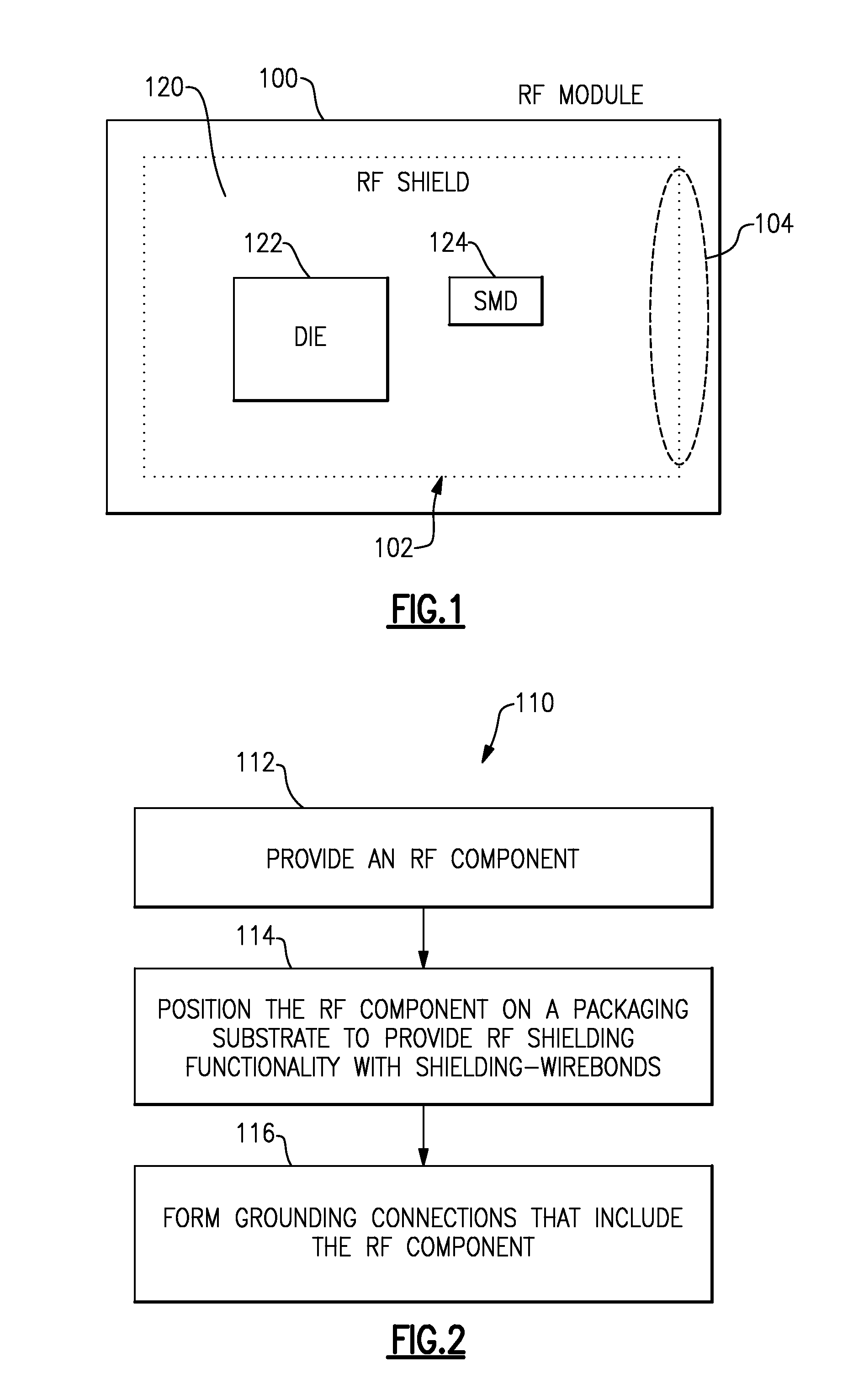
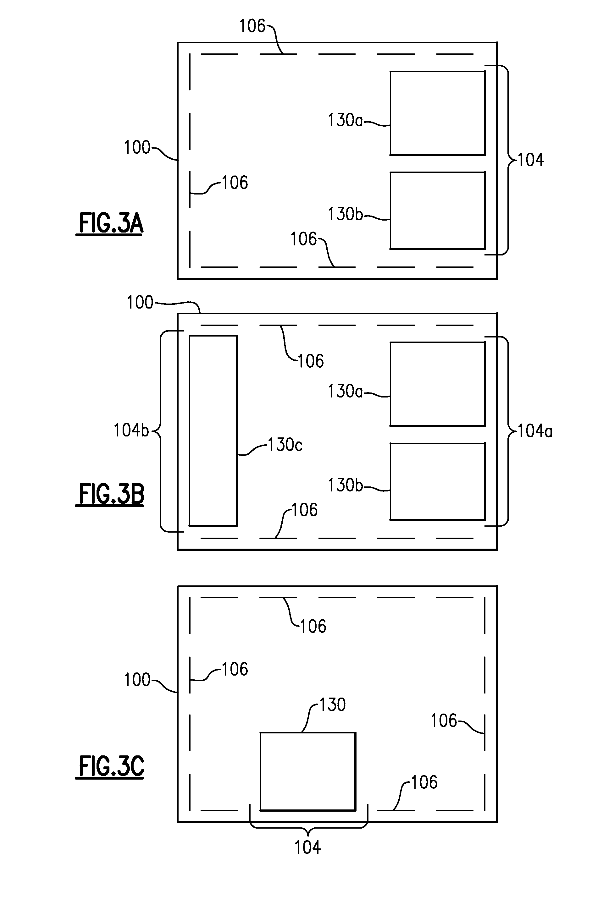
[0058]Disclosed herein are various devices and methods for providing radio-frequency (RF) isolation or shielding for an active or a passive RF device. For the purpose of description, it will be understood that RF can include electromagnetic signals having a frequency or a range of frequencies associated with wireless devices. RF can also include electromagnetic signals that radiate within an electronic device, whether or not such an electronic device operates as a wireless device. RF can also include signals or noises typically associated with electromagnetic interference (EMI) effects.

[0059]For the purpose of description it will be understood that such an RF device can include a device configured to operate at an RF range to facilitate transmitting and / or receiving of RF signals, and a device that can influence another device by, or be inf...


PUM

PropertyMeasurementUnit
angleaaaaaaaaaa
wavelengthaaaaaaaaaa
electricallyaaaaaaaaaa

Abstract

Disclosed are apparatus and methods related to ground paths implemented with surface mount devices to facilitate shielding of radio-frequency (RF) modules. In some embodiments, a module can include a packaging substrate configured to receive a plurality of components. The module can further include an RF component mounted on the packaging substrate and configured to facilitate processing of an RF signal. The module can further include an RF shield disposed relative to the RF component, with the RF shield being configured to provide shielding for the RF component. The RF shield can include at least one shielding-component configured to provide one or more electrical paths between a conductive layer on an upper surface of the module and a ground plane of the packaging substrate. The shielding-component can include a surface-mount device such as an RF filter implemented as a chip size surface acoustic wave (SAW) device (CSSD).

Description

CROSS-REFERENCE TO RELATED APPLICATIONS[0001]This application claims priority to U.S. Provisional Application No. 61 / 812,610 filed Apr. 16, 2013, entitled RADIO-FREQUENCY SHIELD GROUND PATH THROUGH A SURFACE MOUNT DEVICE, and U.S. Provisional Application No. 61 / 817,295 filed Apr. 29, 2013, entitled TIERED PACKAGE-LEVEL RADIO-FREQUENCY SHIELDING, the disclosure of each of which is hereby expressly incorporated by reference herein in its respective entirety.BACKGROUND[0002]1. Field[0003]The present disclosure generally relates to shielding of radio-frequency modules.[0004]2. Description of the Related Art[0005]Electromagnetic (EM) fields can be generated from or have an undesirable effect on a region of a radio-frequency (RF) device such as an RF module. Such an EM interference (EMI) can degrade the performance of wireless devices that use such an RF module. Some RF modules can be provided with EM shields to address such performance issues associated with EMI.SUMMARY[0006]In some impl...

Claims


Application Information

Patent Timeline
Patent Type & Authority Applications(United States)
IPC IPC(8): H05K1/02H04B1/38H05K1/18
CPCH04B1/3838H05K1/0216B23K26/365H05K9/0022H05K1/181H01L21/50H01L23/3114H01L23/3121H05K3/288H05K2201/10287H05K2201/1056H05K2203/107H05K2203/1327H01L2224/4813H01L2224/48227H01L2224/49171H01L2924/19105H01L2924/19107B23K26/40H01L2224/05554B23K26/361B23K26/389H01L24/48H01L2924/00014H01L2224/13025Y10T29/49016Y10T29/49002B23K2103/172H01L2224/73265H01L2924/3025H01L2224/32225H01L2924/00H01L2224/45099B23K26/362B23K26/386H01L21/565H01L21/76802H01L21/76877H01L23/481H01L23/49838H01L23/552H01L23/66H01L24/17H01L24/32H01L24/49H01L24/73H01L2223/6611H01L2223/6616H01L2223/6677H01L2224/16227H01L2224/48091H01L2224/48106H04B1/3833H05K1/183H05K3/30H05K2201/10098H03H9/64H04B1/40H05K1/0218H05K1/0243H05K3/303H05K2201/1006H05K2201/10083
Inventor CHEN, HOWARD E.
Owner SKYWORKS SOLUTIONS INC
Why Eureka
Try Eureka