Wafer level chip size packaged chip device with an N-shape junction inside and method of fabricating the same

a chip device and chip size technology, applied in semiconductor devices, semiconductor/solid-state device details, electrical devices, etc., can solve problems such as cracking of solder ball joints, flip-chip packages, and t-shape junctions that are believed to be rather fragil

Active Publication Date: 2008-07-01
CHINA WAFER LEVEL CSP
View PDF6 Cites 51 Cited by
  • Summary
  • Abstract
  • Description
  • Claims
  • Application Information

AI Technical Summary

Benefits of technology

[0022]In the wafer level chip size packaged chip device of the present invention, with such an n-shape junction instead of a conventional T-shape junction, electrical connections between compatible pads and external leads are more reliable due to larger connection area than the counterpart in the T-shape junction.

Problems solved by technology

The flip-chip package encounters a problem, namely, cracking of solder ball joint due to large thermal expansion mismatch between a wafer and a substrate.
The T-shape junction is believed to be rather fragile, e.g., upon undergoing stress-induced deformation during or after packaging, in terms of electrical connection.

Method used


Image

  • Wafer level chip size packaged chip device with an N-shape junction inside and method of fabricating the same
  • Wafer level chip size packaged chip device with an N-shape junction inside and method of fabricating the same
  • Wafer level chip size packaged chip device with an N-shape junction inside and method of fabricating the same

Examples


Embodiment Construction

[0027]Wherever possible, the same reference numbers are used in the drawings and the description to refer to the same or like parts.

[0028]We follow a whole package process flow, although some process steps of which are exactly the same as that of the standard Shellcase packaging technology, to present the current invention. In this way, it will help one to understand the present invention well.

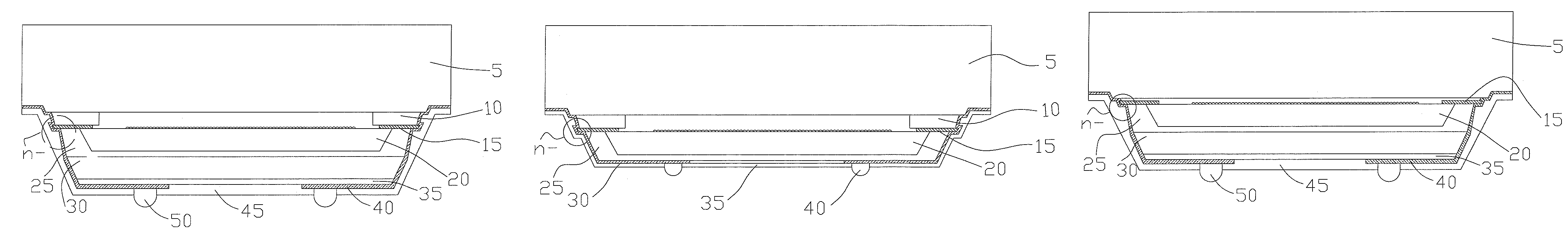
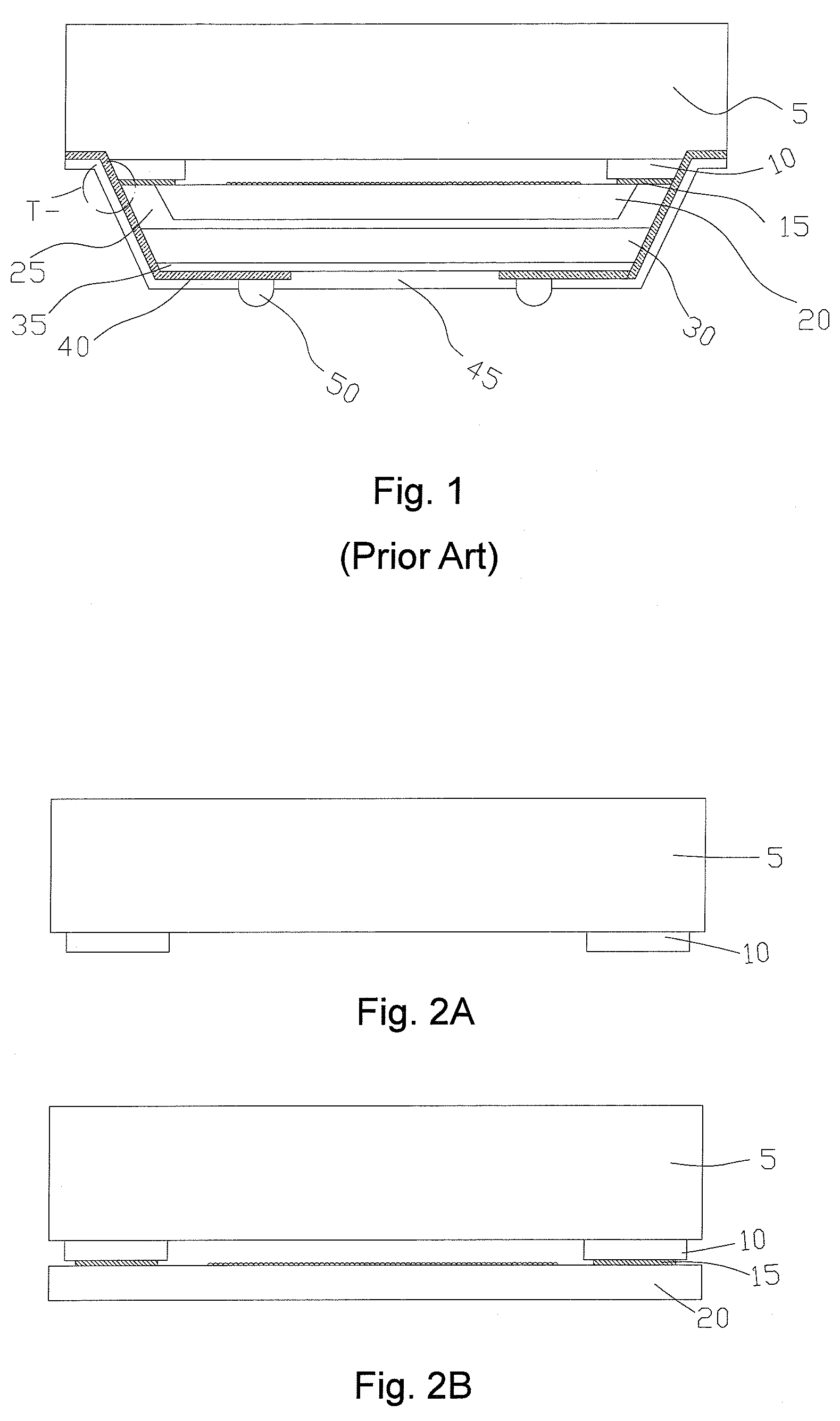
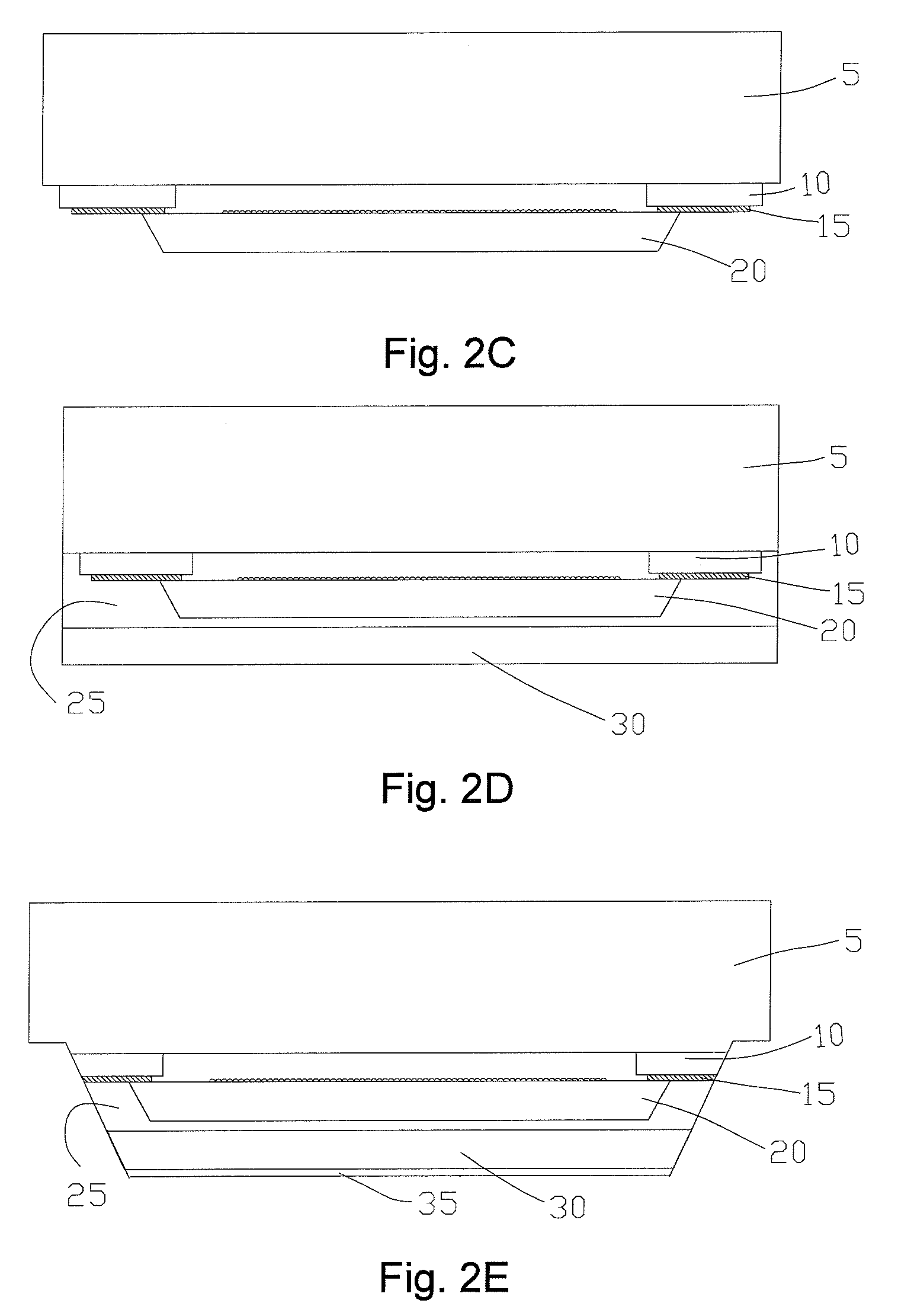
[0029]For one preferred embodiment of this invention based on ShellOC technology, references are made to FIG. 2A-FIG. 2J. As shown, on a first glass 5, cavity walls 10 are formed by photolithography technique (FIG. 2A). The glass 5 with cavity walls 10 formed thereon is applied to cover the silicon chip 20 with optical or image sensors thereof and peripheral arrayed compatible pads 15 thereon (FIG. 2B), wherein an optical / image component (as shadowed) is encased within a cavity, thereby preventing the optical / image component from being contaminated by outside environment. Following this, the c...


PUM


Abstract

The present invention provide a wafer level chip size packaged chip device with a N-shape junction at which external leads electrically connect to peripheral arrayed compatible pads and a method of fabricating the same. In the wafer level chip size package, with such an n-shape junction instead of a conventional T-shape junction observed in Shellcase type wafer level chip size package technology, electrical connections between compatible pads and external leads are more reliable due to larger connection area than the counterpart in the T-shape junction.

Description

FIELD OF THE INVENTION[0001]The present invention relates generally to a wafer level chip size packaging technology, and more particularly to a wafer level chip size packaged chip device that a patterned redistribution metal connects to compatible pads peripherally distributed on silicon chips in the form of n-shape junctions instead of original T-shape junctions for improving the reliability of electrical connection and the method of fabricating such an n-shape junction.BACKGROUND OF THE INVENTION[0002]With the miniaturization of electronic devices and increasing circuit density in semiconductor industry, chip size package (CSP) is developed, where the package size is similar to the semiconductor chip encased within the package. Conventional packaging technologies, wire bonding, tape automatic bonding (TAB) and flip chip, have their own disadvantages. In wire bonding and TAB, a semiconductor package has a footprint much larger than that of the primitive chip. Flip chip package invo...

Claims


Application Information

Patent Timeline
Patent Type & Authority Patents(United States)
IPC IPC(8): H01L31/05
CPCH01L23/3114H01L24/05H01L24/13H01L2224/13022H01L2924/01078H01L2924/10253H01L2924/14H01L2924/00H01L2224/0401
Inventor YU, GUOQINGWANG, YOUJUNXU, QINQINWANG, QINGWEIWANG, WEI
Owner CHINA WAFER LEVEL CSP
Why Eureka
Try Eureka