

Fan-in leadframe semiconductor package
- Summary
- Abstract
- Description
- Claims
- Application Information
AI Technical Summary
Benefits of technology
Problems solved by technology
Method used
Image

Examples
first embodiment
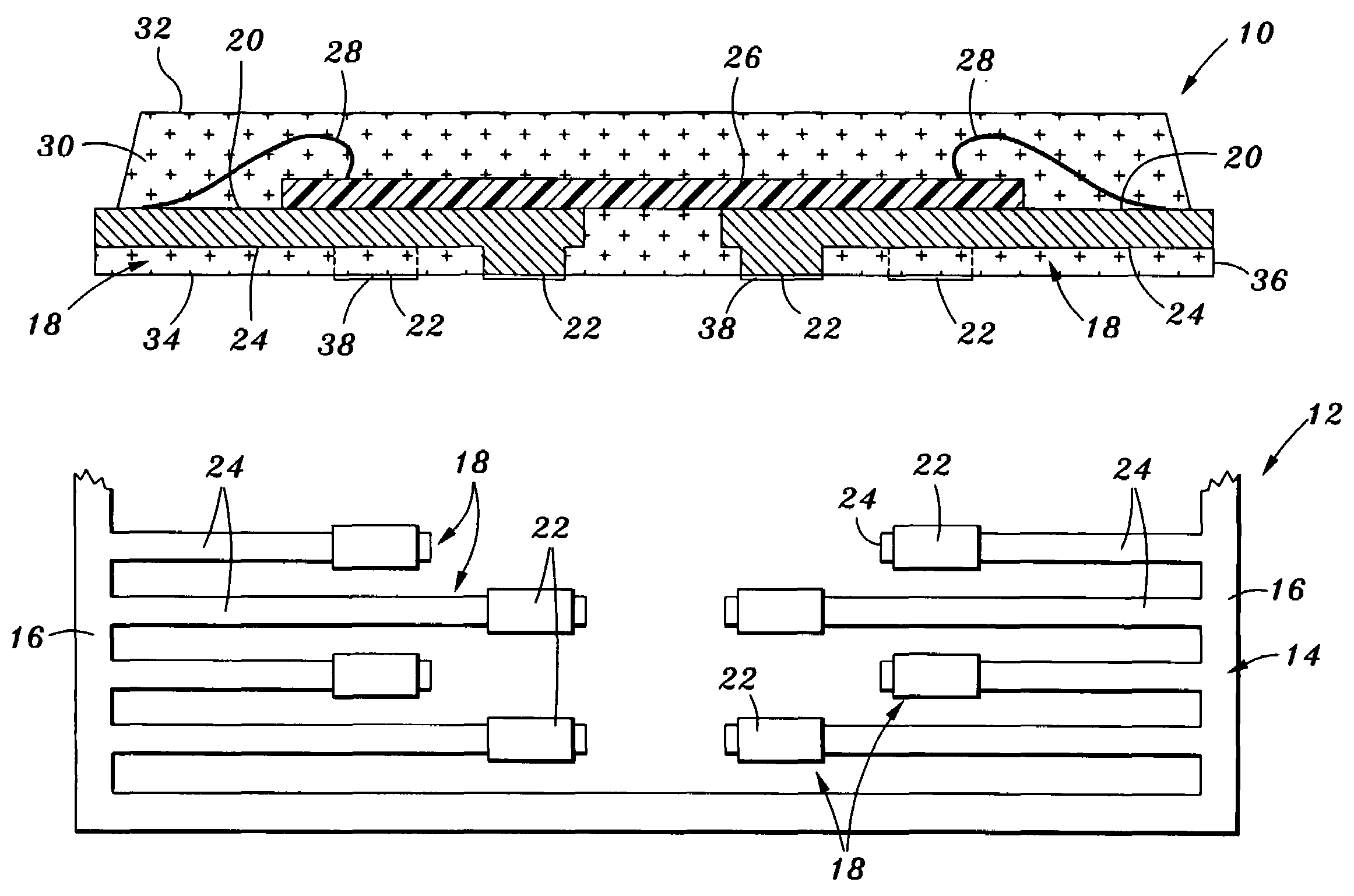
[0017]Referring now to the drawings wherein the showings are for purposes of illustrating preferred embodiments of the present invention only, and not for purposes of limiting the same, FIG. 1 depicts a fan-in semiconductor package 10 constructed in accordance with the present invention. The semiconductor package 10 comprises a fan-in leadframe 12, a partial bottom plan view of which is shown in FIG. 2. The leadframe 12 includes an outer frame 14 having a generally quadrangular (e.g., square, rectangular) configuration. In this regard, the outer frame 14 defines two pairs of opposed sides, with one such pair being labeled with the reference numerals 16 in FIG. 2. Due to the configuration of the outer frame 14, the pair of opposed sides 16 thereof extend in spaced, generally parallel relation to each other.
[0018]As further seen in FIG. 2, integrally connected to and extending inwardly from each of the opposed sides 16 of the outer frame 14 are a plurality of elongate leads 18. In thi...
second embodiment
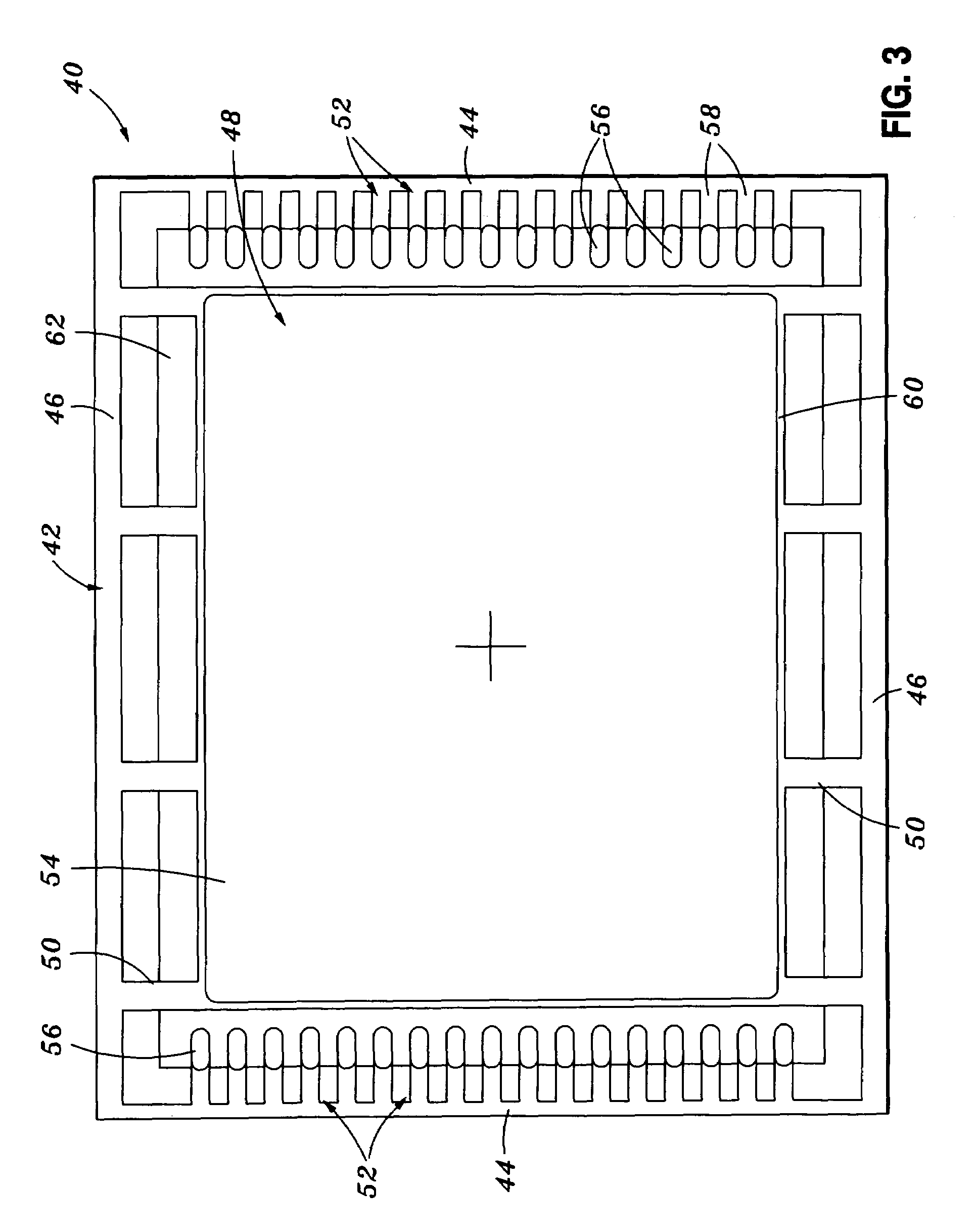
[0025]Referring now to FIG. 3, there is shown a fan-in leadframe 40 constructed in accordance with the present invention. The leadframe 40 includes an outer frame 42 having a generally quadrangular (e.g., square, rectangular) configuration. The outer frame 14 defines two pairs of opposed sides, with one such pair being labeled with the reference numerals 44 in FIG. 3, and the remaining pair being labeled with the reference numerals 46.
[0026]The leadframe 40 includes a generally quadrangular die pad 48 which resides within the interior of the outer frame 46. The die pad 48 is integrally connected to the sides 46 of the outer frame 42 by a plurality of tie bars 50 extending therebetween. Integrally connected to and extending inwardly from each of the opposed sides 44 of the outer frame 42 are a plurality of elongate leads 52. The leads 52 are segregated into two sets, with the leads 52 of each such set being integrally connected to a respective one of the opposed sides 44. The leads 5...
third embodiment
[0034]Referring now to FIG. 4, there is shown a fan-in semiconductor package 70 constructed in accordance with the present invention. The semiconductor package 70 comprises a fan-in leadframe 72, a partial bottom plan view of which is shown in FIG. 5. The leadframe 72 includes an outer frame 74 having a generally quadrangular (e.g., square, rectangular) configuration. In this regard, the outer frame 74 defines two pairs of opposed sides, with one such pair being labeled with the reference numerals 76 in FIG. 5. Due to the configuration of the outer frame 74, the pair of opposed sides 76 thereof extend in spaced, generally parallel relation to each other.
[0035]Integrally connected to and extending inwardly from each of the opposed side 76 of the outer frame 74 are a plurality of elongate leads 78. The leads 78 are segregated into two sets, with the leads 78 of each such set being integrally connected to a respective one of the opposed sides 76. The leads 78 of each set are preferably...
PUM
 Abstract
Description
Claims
Application Information