Multilayer interconnection board, semiconductor device having the same, and method of forming the same as well as method of mounting the semiconductor chip on the interconnection board

a multi-layer interconnection and semiconductor technology, applied in the field of interconnection boards, can solve the problems of high cost of ceramic-based materials, deterioration of temperature cycle characteristics, and high cost of mounting reliability, and achieve high reliability in connection, increase the density of the interconnection board, and reduce the cost

Inactive Publication Date: 2007-05-15
RENESAS ELECTRONICS CORP
View PDF106 Cites 45 Cited by
  • Summary
  • Abstract
  • Description
  • Claims
  • Application Information

AI Technical Summary

Benefits of technology

[0045]It is a still further object of the present invention to provide a novel method of mounting a semiconductor chip on an improved interconnection board allowing a further reduction in the cost thereof.
[0046]It is yet a further object of the present invention to provide a novel method of mounting a semiconductor chip on an improved interconnection board free of any bend.
[0047]It is further more object of the present invention to provide a novel method of mounting a semiconductor chip on an improved interconnection board allowing a high reliability in connection between the interconnection board and a semiconductor chip.
[0048]It is moreover object of the present invention to provide a novel method of mounting a semiconductor chip on an improved interconnection board allowing a further increase in density of the interconnection board.
[0049]It is still more object of the present invention to provide a novel method of mounting a semiconductor chip on an improved interconnection board allowing a further reduction in an external size of the interconnection board.
[0050]It is yet more object of the present invention to provide a novel method of mounting a semiconductor chip on an improved interconnection board free from a deterioration in reliability of connection between the interconnection board and a circuit board on which the interconnection board is mounted.

Problems solved by technology

The above conventional technique is disadvantageous in deteriorated mounting reliability, particularly deteriorated temperature cycle characteristics.
The use of the ceramic-based material is effective in improvement in reliability of mounting the flip-chip semiconductor chip 101 on the multilayer interconnection board 103, but disadvantageous as the ceramic-based material is expensive.
The application of this conventional technique is limited to supercomputers and large scale computers.
However, the glass epoxy resin base material has a large difference in thermal expansion coefficient from the semiconductor chip, whereby a large stress is applied between the multilayer interconnection board of the glass epoxy resin base material and the semiconductor chip thereby to drop the reliability in connection between the multilayer interconnection board and the semiconductor chip.
This limitation to minimize the pitch of the above multilevel interconnection patterns makes it difficult to further increase the density of the multilayer interconnection board and further reduce the external size of the multilayer interconnection board.
Consequently, the multilayer interconnection board of the glass epoxy resin base material makes it difficult to further increase the density of the multilayer interconnection board and further reduce the external size of the multilayer interconnection board.
This makes it difficult to further reduce the cost of the multilayer interconnection board.
Furthermore, when the multilayer interconnection board with the semiconductor chip is mounted on a circuit board, a stress is applied between the multilayer interconnection board and the circuit board due to a difference in thermal expansion coefficient between the multilayer interconnection board and the circuit board, thereby deteriorating a reliability in connection between the multilayer interconnection board and the circuit board.

Method used


Image

  • Multilayer interconnection board, semiconductor device having the same, and method of forming the same as well as method of mounting the semiconductor chip on the interconnection board
  • Multilayer interconnection board, semiconductor device having the same, and method of forming the same as well as method of mounting the semiconductor chip on the interconnection board
  • Multilayer interconnection board, semiconductor device having the same, and method of forming the same as well as method of mounting the semiconductor chip on the interconnection board

Examples


first embodiment

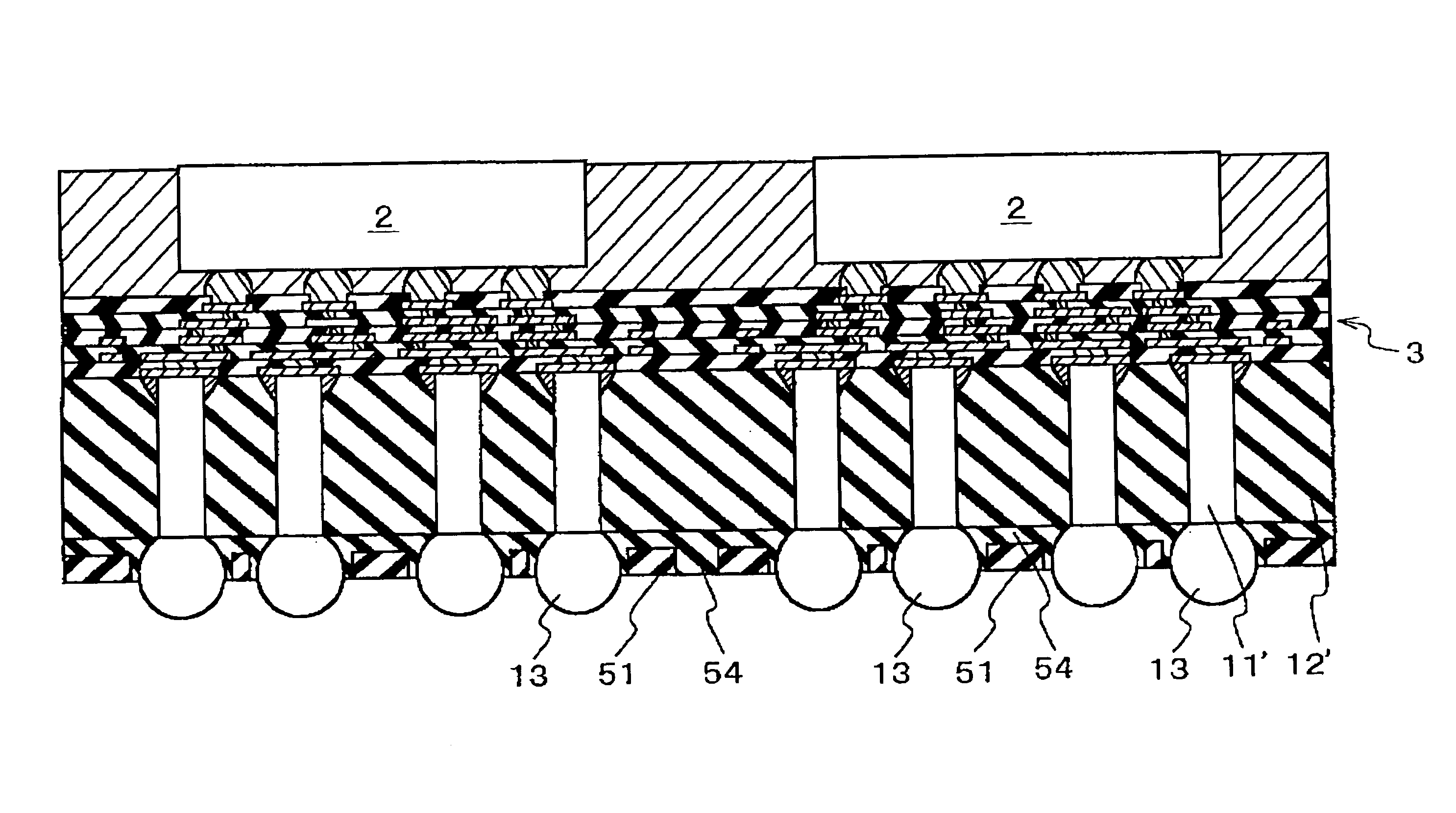
[0151]A first embodiment according to the present invention will be described in detail with reference to the drawings. FIG. 4 is a cross sectional elevation view illustrative of a semiconductor device having a multilayer interconnection board, on which a semiconductor chip is mounted in a first embodiment according to the present invention. A semiconductor device 32 has a multilayer interconnection board 3. A flip-chip semiconductor chip 2 is flip-mounted on the multilayer interconnection board 3, wherein a first surface of the flip-chip semiconductor chip 2 is electrically connected through bumps 14 to a first surface of the multilayer interconnection board 3. A second surface of the multilayer interconnection board 3 has arrays of external electrode pads 17 on which solder balls 13 are formed. A sealing resin material 15 is provided over the first surface of the multilayer interconnection board 3 for sealing the semiconductor chip 2 and the bumps 14. A heat conductive adhesive la...

second embodiment

[0192]A second embodiment according to the present invention will be described in detail with reference to the drawings. The second embodiment is different from the first embodiment only in the fabrication processes for the flip-chip semiconductor device 32, for which reason the following descriptions will focus on the fabrication processes and the description of the structure of the flip-chip semiconductor device 32 will be omitted.

[0193]FIGS. 8A through 8Q are fragmentary cross sectional elevation views illustrative of a novel method of forming a semiconductor device having a multilayer interconnection board on which a semiconductor chip is mounted in a second embodiment in accordance with the present invention.

[0194]With reference to FIG. 8A, a high rigidity plate 16 is prepared. The high rigidity plate 16 may be made of any material having a high rigidity. Metals such as Cu-, Ni-, Al-, W-, Mo-, Au-, Ag- and Pt-based metals, complex materials of different metals and ceramics are ...

third embodiment

[0228]A third embodiment according to the present invention will be described in detail with reference to the drawings. The third embodiment is different from the first embodiment only in the fabrication processes for the flip-chip semiconductor device 32, for which reason the following descriptions will focus on the fabrication processes and the description of the structure of the flip-chip semiconductor device 32 will be omitted.

[0229]FIGS. 9A through 9P are fragmentary cross sectional elevation views illustrative of a novel method of forming a semiconductor device having a multilayer interconnection board on which a semiconductor chip is mounted in a third embodiment in accordance with the present invention.

[0230]With reference to FIG. 9A, a high rigidity plate 16 is prepared. The high rigidity plate 16 may be made of any material having a high rigidity. Metals such as Cu-, Ni-, Al-, W-, Mo-, Au-, Ag- and Pt-based metals, complex materials of different metals and ceramics are ava...


PUM


Abstract

In accordance with the present invention, during formation of the interconnection board, the interconnection board remains securely fixed to a high rigidity plate being higher in rigidity than the interconnection board for suppressing the interconnection board from being bent.

Description

BACKGROUND OF THE INVENTION[0001]The present invention relates to an interconnection board, a semiconductor device having an interconnection board, a method of forming the interconnection board and a method of mounting the semiconductor chip on the interconnection board, and more particularly to a multilayer interconnection board for allowing a flip-chip semiconductor chip to be mounted thereon, a semiconductor device having a multilayer interconnection board, a method of forming the multilayer interconnection board and a method of mounting the flip-chip semiconductor chip on the multilayer interconnection board.[0002]In recent years, the importance of the flip-chip semiconductor chip for realizing the high density package has been on the increase. FIG. 1 is a schematic cross sectional elevation view illustrative of a flip-chip semiconductor chip. A flip-chip semiconductor chip 101 has a first surface which further has a predetermined area array of external terminals not illustrated...

Claims


Application Information

Patent Timeline
Patent Type & Authority Patents(United States)
IPC IPC(8): H01L23/34H01L23/48H01L23/52H01L29/40H01L23/12H01L21/48H01L21/60H01L21/68H01L23/00H01L23/31H01L23/498H05K3/20H05K3/46
CPCH01L21/486H01L21/6835H01L23/3121H01L23/49811H01L23/49816H01L23/49822H01L23/49827H01L23/562H01L24/97H05K3/467H05K3/4682H01L2221/68345H01L2221/68377H01L2224/16225H01L2224/16227H01L2224/73253H01L2224/81001H01L2224/97H01L2924/01002H01L2924/01004H01L2924/01013H01L2924/01015H01L2924/01027H01L2924/01029H01L2924/0103H01L2924/01033H01L2924/01042H01L2924/01046H01L2924/01047H01L2924/01074H01L2924/01075H01L2924/01077H01L2924/01078H01L2924/01079H01L2924/01082H01L2924/09701H01L2924/15311H01L2924/15312H01L2924/16195H01L2924/18161H05K3/20H01L2224/81H01L2924/01005H01L2924/01006H01L2924/01023H01L2924/01024H01L2224/32225H01L2224/73204H01L2924/00Y10S438/977H01L2224/29099H01L2924/00013H01L2224/32245H01L2224/81005H01L2924/12042H01L2924/351H01L23/12
Inventor HONDA, HIROKAZU
Owner RENESAS ELECTRONICS CORP
Why Eureka
Try Eureka