

Squelch detecting circuit
a detection circuit and circuit technology, applied in the direction of electrical equipment, gain control, baseband system details, etc., can solve the problems of reducing signal amplitude, physical limitations, and processing large amounts of digital data, so as to reduce reduce power consumption and parts cost. , the effect of reducing the number of high-speed operating operational amplifiers
- Summary
- Abstract
- Description
- Claims
- Application Information
AI Technical Summary
Benefits of technology
Problems solved by technology
Method used
Image

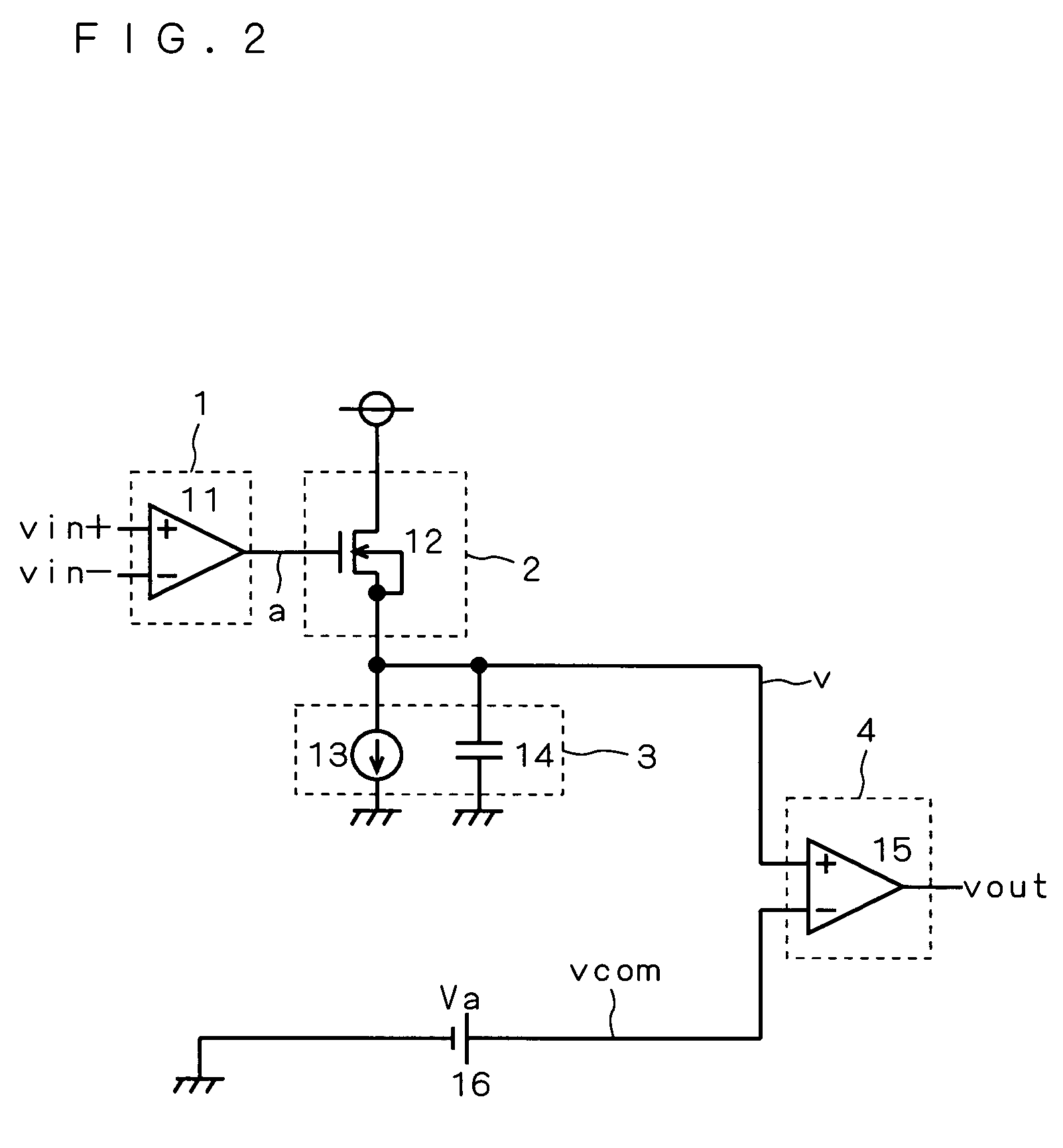
Examples
first modification
[0082](First Modification)
[0083]FIG. 12 is a circuit diagram of the squelch detecting circuit according to a first modification of this preferred embodiment. This modification uses a replica circuit 60 in place of the constant-voltage source 16 of the modification of the first preferred embodiment. In FIG. 12, the operational amplifier 11 amplifies the input differential signals to output a single-end amplified signal. The single-end amplified signal outputted from the operational amplifier 11 is applied to the gate electrode of the p-channel transistor 21. The p-channel transistor 21 supplies to the current source 13 and capacitance 14 a potential proportional to the applied amplified signal. The current source 13 and the capacitance 14 each have one terminal connected to the source electrode of the p-channel transistor 21 and the other terminal connected to power-supply. The potential held by the current source 13 and the capacitance 14 is supplied to the minus terminal of the ope...
second modification
[0086](Second Modification)
[0087]FIG. 14 is a circuit diagram of the squelch detecting circuit according to a second modification. This modification uses a replica circuit 70 in place of the constant-voltage source 16 of the second preferred embodiment. In FIG. 14, the operational amplifier 31 amplifies the input differential signals to output differential amplified signals. One of the differential amplified signals that is outputted from the minus side of the operational amplifier 31 is applied to the gate electrode of the n-channel transistor 32. The other differential amplified signal outputted from the plus side of the operational amplifier 31 is applied to the gate electrode of the n-channel transistor 33. The n-channel transistor 32 and the n-channel transistor 33 supply the current source 34 and capacitance 35 with potential proportional to the applied amplified signals. The current source 34 and the capacitance 35 each have one terminal connected to the source electrodes of ...
third modification
[0090](Third Modification)
[0091]FIG. 16 is a circuit diagram of the squelch detecting circuit according to a third modification. This modification uses a replica circuit 80 in place of the constant-voltage source 16 of the modification of the second preferred embodiment. In FIG. 16, the operational amplifier 31 amplifies the input differential signals to output differential amplified signals. One of the differential amplified signals that is outputted from the plus side of the operational amplifier 31 is applied to the gate electrode of the p-channel transistor 41. The other differential amplified signal outputted from the minus side of the operational amplifier 31 is applied to the gate electrode of the p-channel transistor 42. The p-channel transistor 41 and the p-channel transistor 42 supply the current source 34 and capacitance 35 with potential proportional to the applied amplified signals. The current source 34 and the capacitance 35 each have one terminal connected to the sou...
PUM
 Abstract
Description
Claims
Application Information