Semiconductor wafer and semiconductor device provided with columnar electrodes and methods of producing the wafer and device

a technology of semiconductor devices and semiconductor wafers, which is applied in the direction of semiconductor devices, semiconductor/solid-state device details, electrical apparatus, etc., can solve the problems of resin left on the top face of the columnar electrode b>24/b> not always fully removed, and achieve the effect of high reliability

Inactive Publication Date: 2007-05-22
SHINKO ELECTRIC IND CO LTD
View PDF10 Cites 91 Cited by
  • Summary
  • Abstract
  • Description
  • Claims
  • Application Information

AI Technical Summary

Benefits of technology

[0013]The invention is intended to solve such prior problems, and an object of the invention is to provide a semiconductor wafer provided with columnar electrodes which can be s

Problems solved by technology

However, merely by peeling the encapsulating film 30 from the encapsulated semiconductor wafer 10, the resin left on the top face of the columnar electrode 24 is not always fully removed.
However, the resin left on the top face of the columnar electrode 24 cannot always be fully removed even by such cleaning, and excessive cleaning to completely remove the resin from the top face of

Method used


Image

  • Semiconductor wafer and semiconductor device provided with columnar electrodes and methods of producing the wafer and device
  • Semiconductor wafer and semiconductor device provided with columnar electrodes and methods of producing the wafer and device
  • Semiconductor wafer and semiconductor device provided with columnar electrodes and methods of producing the wafer and device

Examples


Embodiment Construction

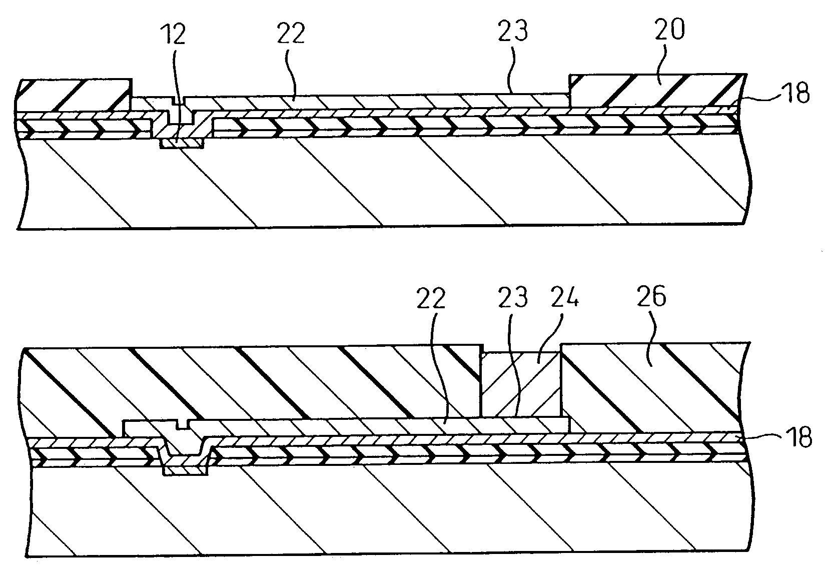
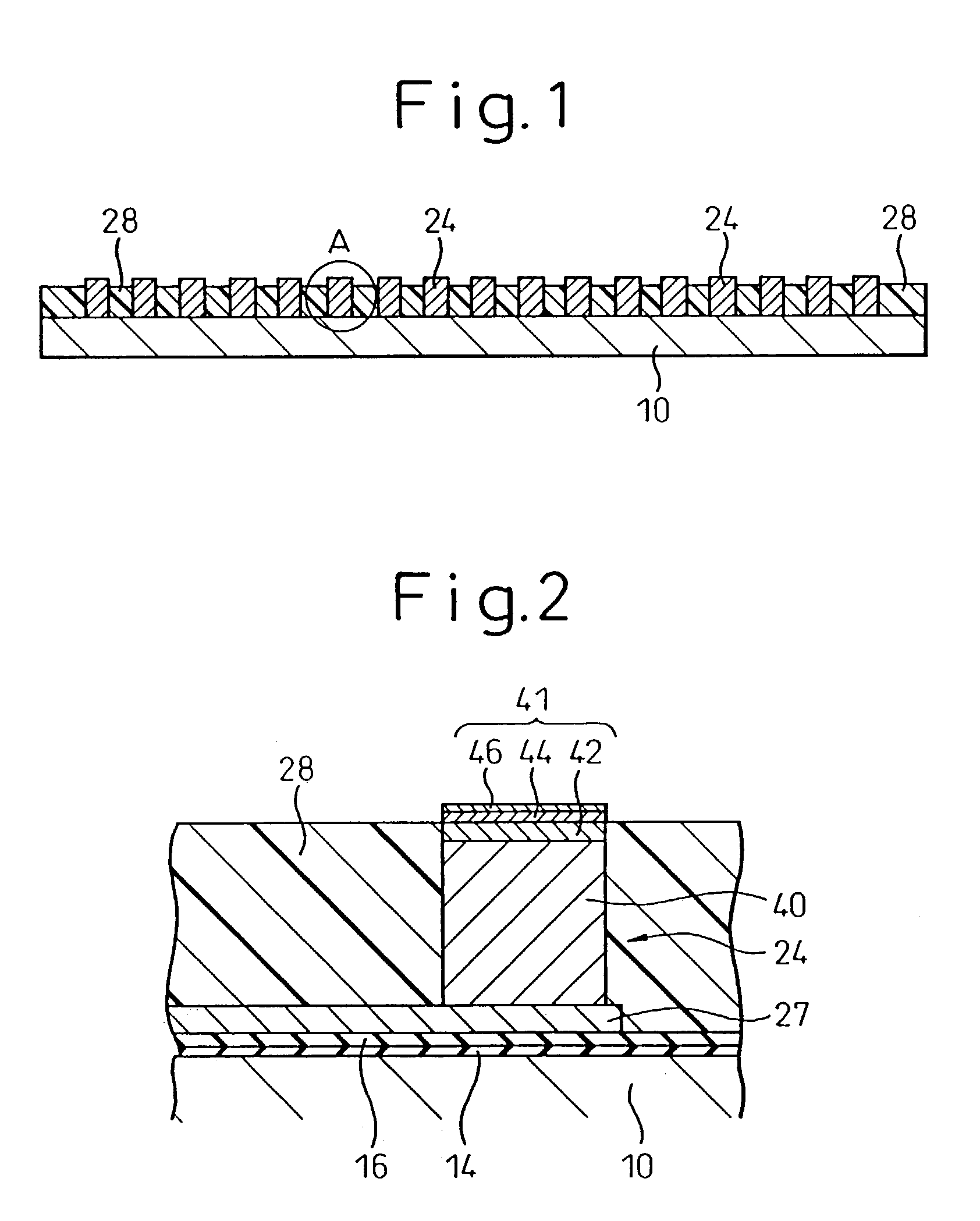
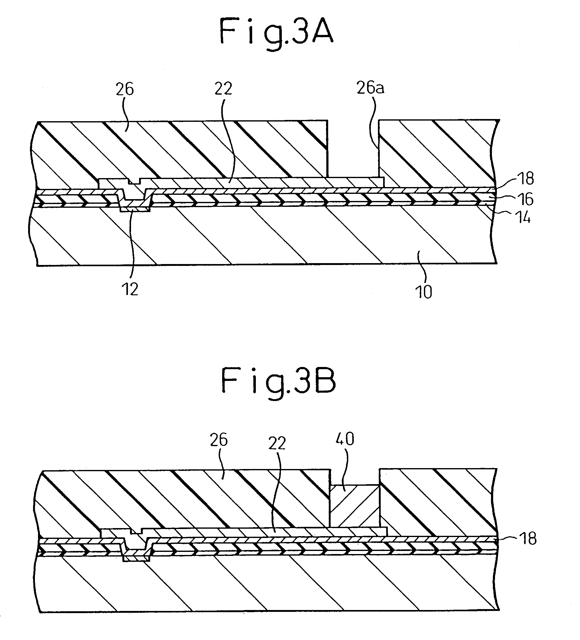
[0041]Referring to FIGS. 1 and 2, an embodiment of the semiconductor wafer of the invention, which is characterized by its columnar electrodes, is described. This semiconductor wafer has the same constitution as that of the prior semiconductor wafer formerly described except for the plated films successively formed at the top of the columnar electrodes. Accordingly, the following description mainly covers the structure associated with the plated films at the top of the columnar electrode, and members which are the same as those of the prior semiconductor wafer formerly illustrated referring to FIG. 11 are identified by the same reference numbers.

[0042]As illustrated in FIG. 1, which schematically shows the entire semiconductor wafer 10 provided with columnar electrodes 24 according to the invention, and FIG. 2, which is a partially enlarged view of the portion indicated by A in FIG. 1, the semiconductor wafer 10 of the invention comprises a passivation film 14 formed on the surface ...


PUM


Abstract

A semiconductor wafer provided with columnar electrodes which have plated nickel, palladium, and gold films successively formed at the top thereof, or have a plated solder film at their top. The semiconductor wafer can be preferably used for producing a chip-sized semiconductor device provided with columnar electrodes to which an external connection terminal, such as a solder ball, is to be bonded. Methods of producing the semiconductor wafer and device by use of plating are also disclosed.

Description

[0001]This application is a divisional of U.S. Ser. No. 09 / 492,094, filed Jan. 27, 2000 now abandoned, which claims priority from Japanese Nos. 11-18229 and 11-18237, both filed in Japan on Jan. 27, 1999.BACKGROUND OF THE INVENTION[0002]1. Field of the Invention[0003]The invention relates to a semiconductor wafer provided with columnar electrodes used for manufacturing semiconductor devices having a size which is approximately the same as a size of a chip sliced from the wafer, which are also called chip-sized packages, and a method of the production such a semiconductor wafer. The invention also related to a semiconductor device provided with columnar electrodes and a method of manufacturing the device.[0004]2. Description of the Related Art[0005]FIGS. 11A to 11G illustrate a method of producing a semiconductor wafer, provided with columnar electrodes, used for manufacturing chip-sized packages. FIG. 11A shows a partially enlarged section of a semiconductor wafer 10, on which elect...

Claims


Application Information

Patent Timeline
IPC IPC(8): H01L21/283H01L21/60H01L23/485
CPCH01L24/11H01L24/13H01L2224/1146H01L2224/1147H01L2224/11849H01L2224/13099H01L2924/01015H01L2924/01027H01L2924/01029H01L2924/01033H01L2924/01046H01L2924/01047H01L2924/01078H01L2924/01079H01L2924/01082H01L2924/01005H01L2924/014H01L2224/131H01L2924/0001H01L2224/05008H01L2224/05026H01L2224/05001H01L2224/05569H01L24/03H01L24/05H01L2224/023H01L2224/05644H01L2924/00014H01L2224/05647H01L2224/05655H01L2224/05664H01L2224/05147H01L2224/05155H01L2224/05164H01L2924/013H01L21/60
Inventor IHARA, YOSHIHIROKOBAYASHI, TSUYOSHIWAKABAYASHI, SHINICHI
Owner SHINKO ELECTRIC IND CO LTD
Why Eureka
Try Eureka