
Image processing device

a processing device and image technology, applied in the field of image processing devices, can solve the problems of insufficient image contrast, and achieve the effects of selectively highlighting, increasing dynamic range, and enhancing contras

Inactive Publication Date: 2007-05-22
HONDA MOTOR CO LTD
View PDF8 Cites 7 Cited by
  • Summary
  • Abstract
  • Description
  • Claims
  • Application Information

AI Technical Summary

Benefits of technology

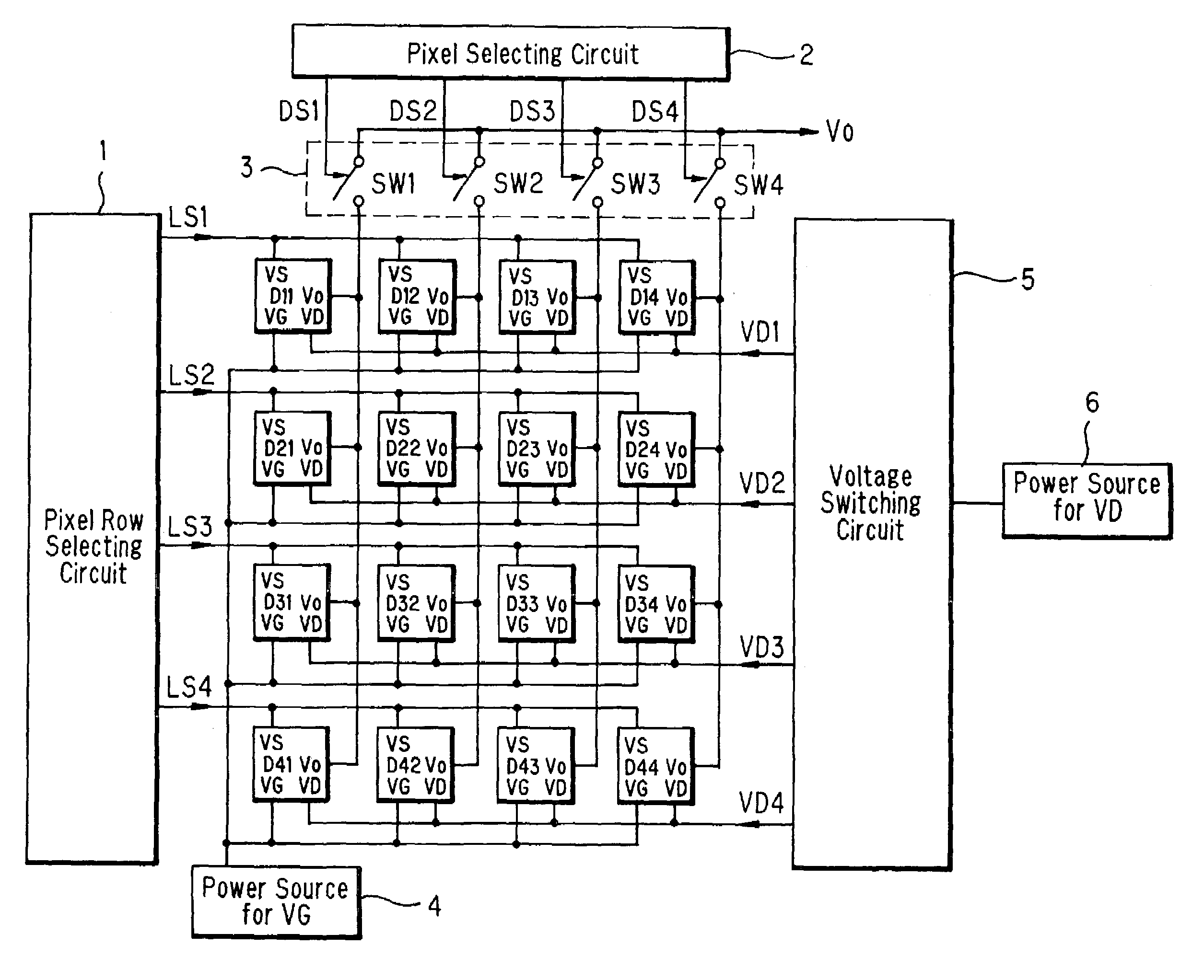
[0007]An object of the present invention is to provide an image processing device capable of emphasizing the contrast of a specified luminance portion of an image taken by an image sensor having a logarithmic output characteristic with an increased dynamic range, which has a means for selectively emphasizing an image sensor output in any plural luminance range by using an output characteristic conversion table so as to increase the contrast of each image portion in any luminance areas of the image output by the image sensor.

Problems solved by technology

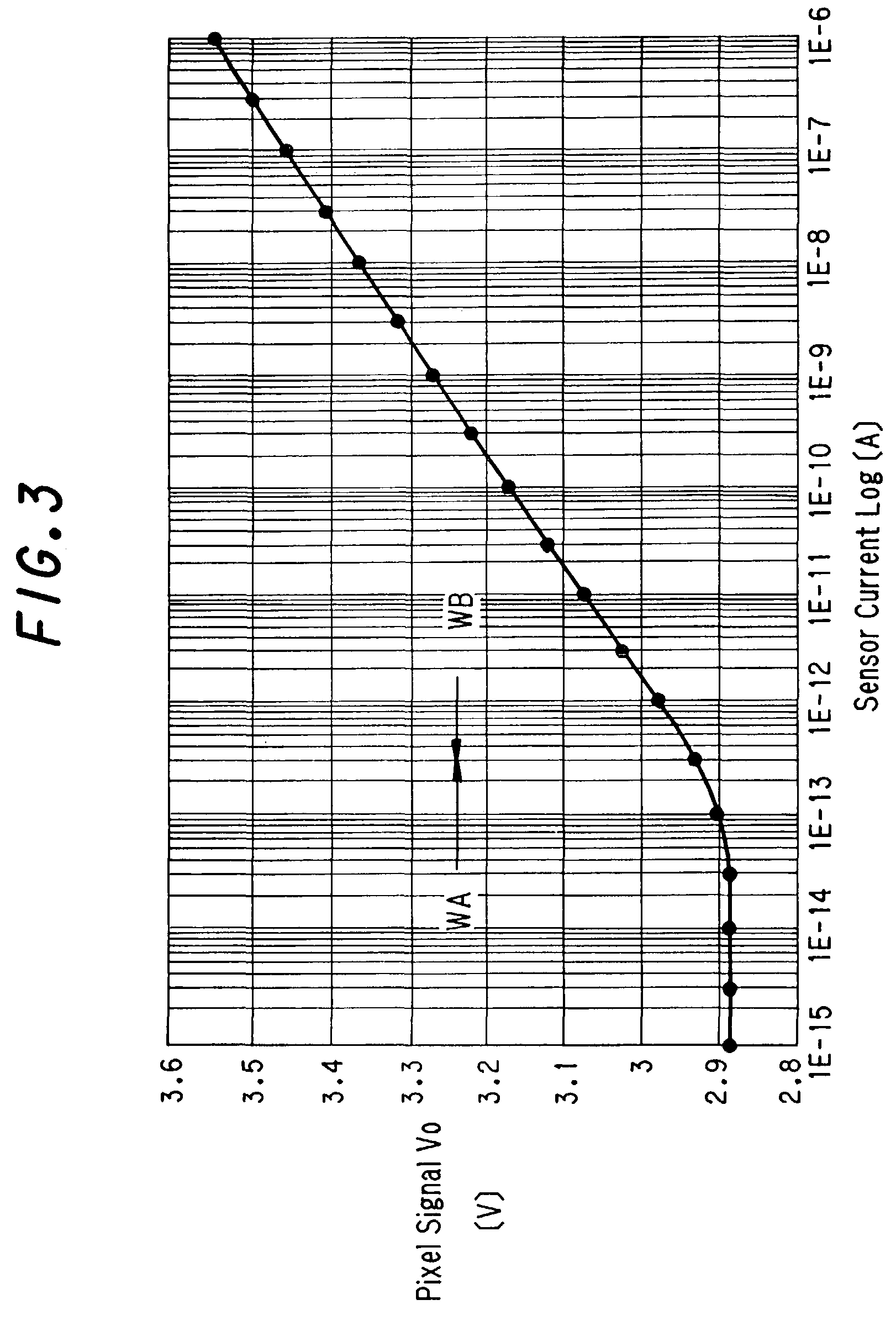
However, the image sensor using light-sensor circuits having a logarithmic output characteristic for attaining a wide dynamic range can take an image covering a wide range from a high bright portion to a dark portion but it may suffer insufficient contrast of the image because of logarithmic compression of luminance.

Method used


Image

  • Image processing device
  • Image processing device
  • Image processing device

Examples


Embodiment Construction

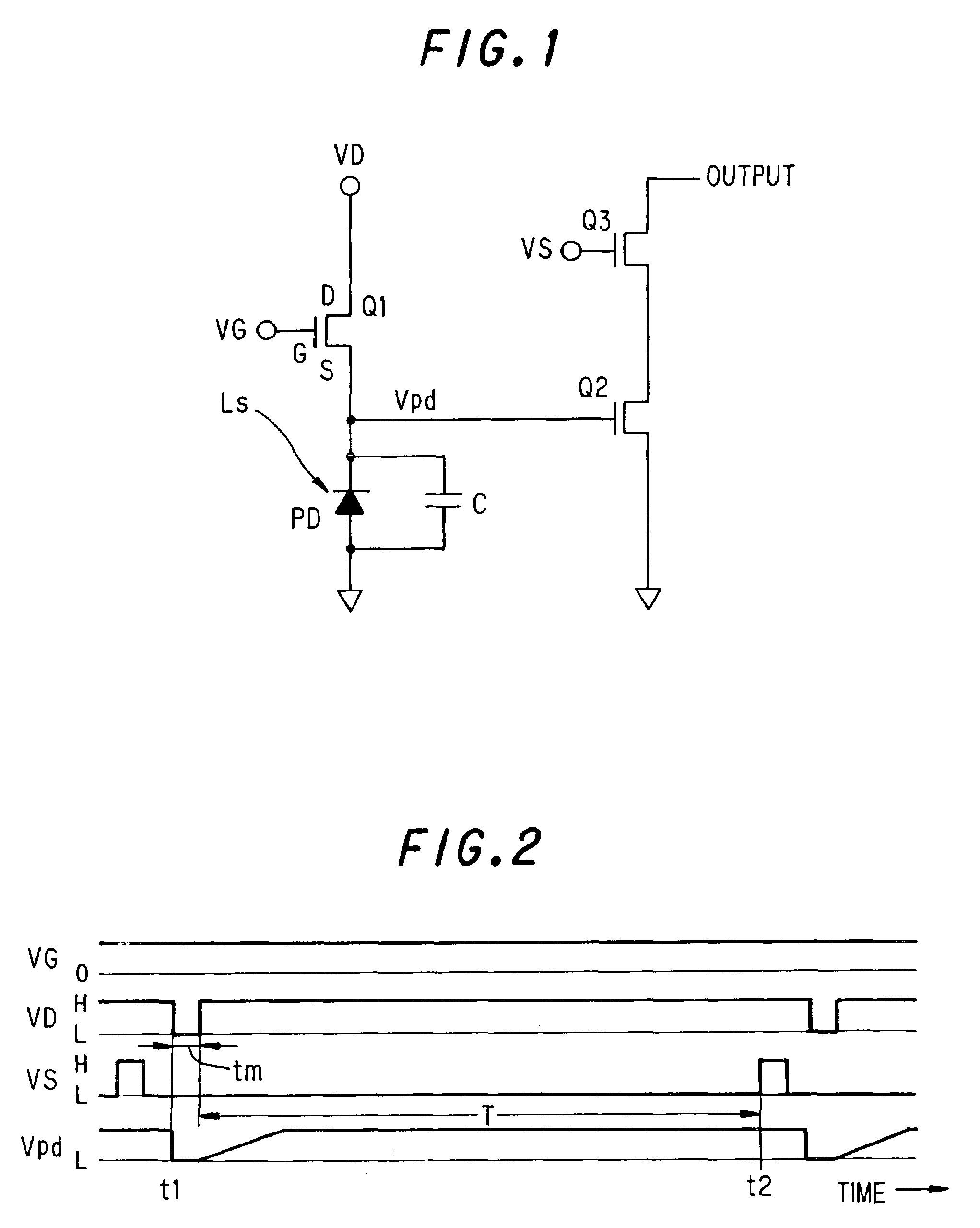
[0035]FIG. 1 illustrates a light sensor circuit representing a unit pixel, which is used as a unit component in an image sensor to which the present invention relates.

[0036]The light sensor circuit can produce a sensor current in the transistor Q1 while a sufficient quantity of light Ls is falling on the photodiode PD and can therefore detect a light signal at a response speed sufficient not to produce an afterimage of the pixel owing to a relatively small value of resistance of the transistor Q1. However, since the transistor Q1 is set to operate with resistance increased by one order when a current therein decreases by one order, decreasing the current flowing in the transistor Q1 with a decrease in the quantity of incident light Ls falling on the photodiode PD causes the transistor Q1 to rapidly increase its resistance. At the same time, a time constant of the circuit containing a parasitic capacitor C of the photodiode PD with the increased resistance is increased to elongate th...


PUM


Abstract

An image processing device for emphasizing a specified luminance area of an image taken by an image sensor. The contrast between a bright portion and a dark portion of an image taken by the image sensor having a wide dynamic range of a logarithmic output characteristic can be increased by selectively emphasizing the image sensor output of any luminance area by using an output characteristic conversion table.

Description

BACKGROUND OF THE INVENTION[0001]The present invention relates to an image processing device for emphasizing a specified luminance portion of an image taken by an image sensor.[0002]Usually, in the case of taking a picture of an object having a bright objective portion (high light portion) and a dark surrounding portion (shadow portion) such as for example a road viewed toward the outlet (or the inlet) of a tunnel from the inside (or the outside) thereof for monitoring a white line marked on the road in front of a vehicle running thereon or an image of a working site where welding, laser machining or plasma machining is conducted, it is highly required to use an image sensor having a sufficiently wide dynamic range.[0003]Referring to FIG. 27, there is shown a state of a weld joint being formed by the laser beam welding on a metal surface where the weld portion comprises a key hole, a molten pool formed by heating with a laser beam at a high temperature and a bead portion formed by s...

Claims


Application Information

Patent Timeline
Patent Type & Authority Patents(United States)
IPC IPC(8): G06K9/40G06T5/00H01L27/146H04N5/20H04N7/18H04N23/76H04N25/00
CPCH04N5/235H04N5/2355H04N5/243H04N5/35518H04N23/70H04N23/741H04N23/76H04N25/573
Inventor SHINOTSUKA, SUKEYUKISEKI, HIDEO
Owner HONDA MOTOR CO LTD
Learn More