Semiconductor devices and methods

a technology of semiconductors and devices, applied in the field of semiconductor devices, can solve the problems of poor qd-to-qd coupling, lack of uniformity, and qd structure that is not uniform, and achieves the effect of optimizing emission and poor qd-to-qd coupling

Inactive Publication Date: 2007-06-05
THE BOARD OF TRUSTEES OF THE UNIV OF ILLINOIS +1
View PDF19 Cites 3 Cited by
  • Summary
  • Abstract
  • Description
  • Claims
  • Application Information

AI Technical Summary

Benefits of technology

[0006]A major problem with quantum dot heterostructures (QDHs) is the stochastic nature of QD structures, the lack of uniformity, insufficient QD density, and poor QD-to-QD coupling. In accordance with an aspect hereof, a solution to the problem is to couple, via a thin barrier, the sheet (or multiple sheets) of QDs to a QW layer, e.g., to the QW layer of a QW laser. The higher energy states of the QDs are resonant with and couple by tunneling to the lower confined-particle states of the thin uniform QW layer. Electron-hole transport in the Q...

Problems solved by technology

A major problem with quantum dot heterostructures (QDHs) is the stochastic nature of ...

Method used


Image

  • Semiconductor devices and methods
  • Semiconductor devices and methods
  • Semiconductor devices and methods

Examples


Embodiment Construction

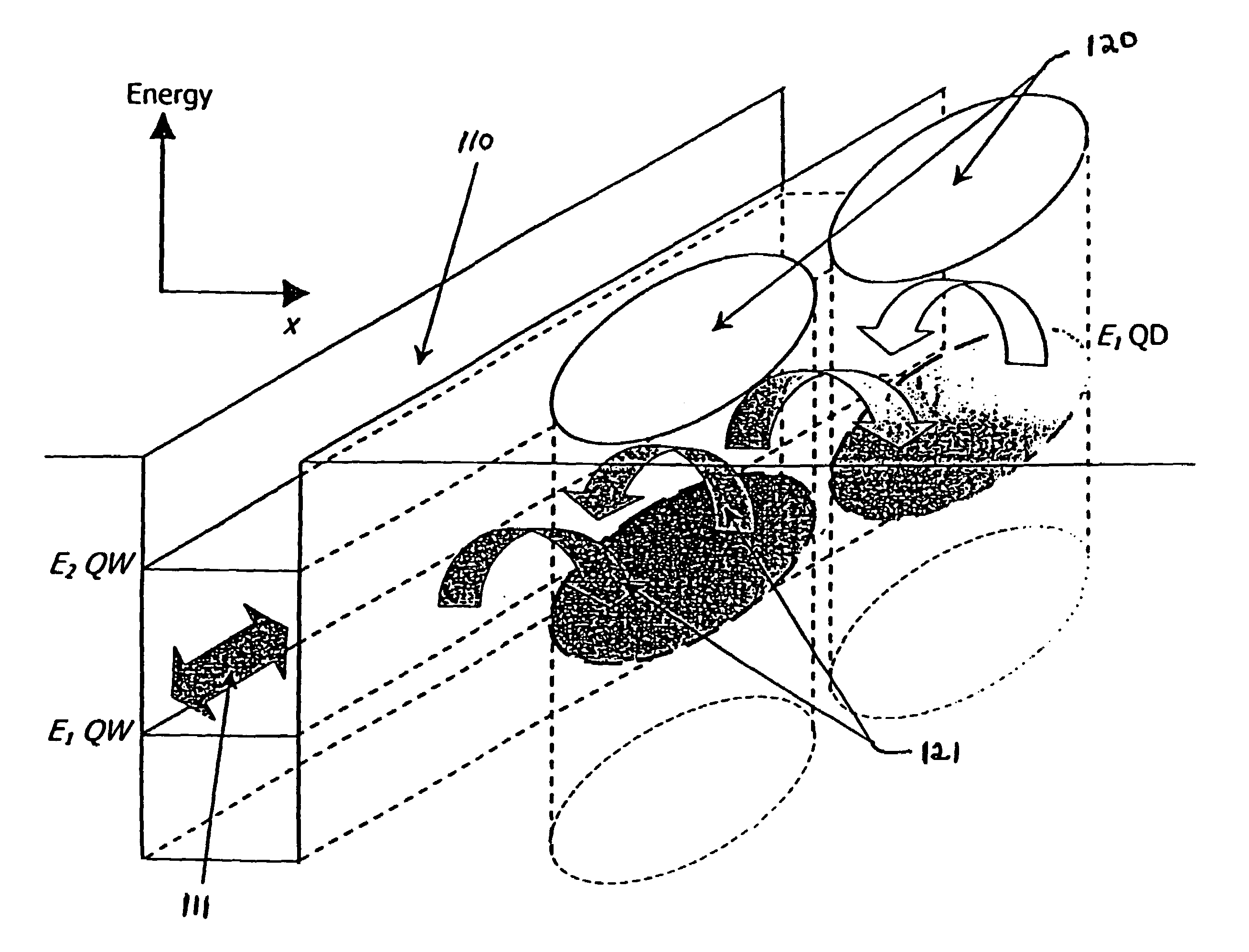
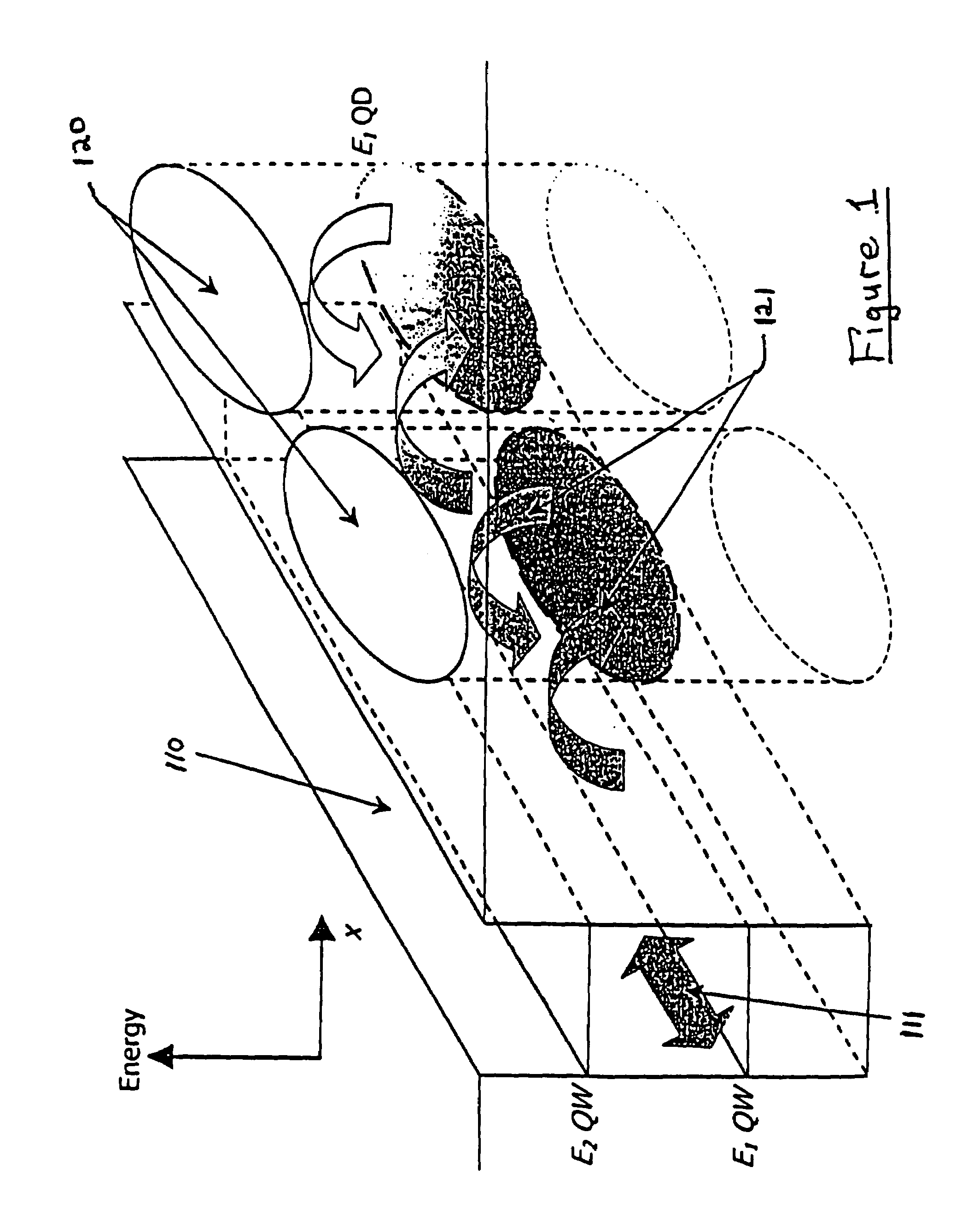
[0028]FIG. 1 is a diagram illustrating intra-QW carrier transport, and inter-QD-QW transport (in both directions) by tunnelling of carriers in a device with a quantum dot layer disposed in close proximity to a quantum well layer. In FIG. 1, the vertical direction represents energy level, and the x direction is normal to the plane of the device layers. The quantum well communication layer is represented at 110, and quantum dots are represented at 120. Quantum well energy states are labelled at E1QW and E2QW, and quantum dot energy state is labelled at E1QD. Double-headed arrow III represents intra QW transport, and the arrows 121 represent inter QW-QD transport in both directions. As seen from the diagram, an electron can, for example, tunnel from quantum dot to the quantum well layer, transports in the quantum well layer, and re-tunnels back into another quantum dot. In this manner, it is possible for the charge to get unstuck from a quantum dot and move from dot to dot in the waveg...


PUM


Abstract

A method of forming a semiconductor device includes the following steps: providing a plurality of semiconductor layers; providing means for coupling signals to and/or from layers of the device; providing a quantum well disposed between adjacent layers of the device; and providing a layer of quantum dots disposed in one of the adjacent layers, and spaced from the quantum well, whereby carriers can tunnel in either direction between the quantum well and the quantum dots.

Description

RELATED APPLICATION[0001]The present Application is a divisional of U.S. patent application Ser. No. 10 / 209,279, filed Jul. 31, 2002, now U.S. Pat. No. 6,753,273 which claims priority from U.S. Provisional Application 60 / 309,149, filed Jul. 31, 2001, and said Provisional Application is hereby incorporated by reference.[0002]This invention was made with Government support, and the Government has certain rights in this invention.FIELD OF THE INVENTION[0003]This invention relates to the field of semiconductor devices and methods of making same, and, more particularly, to a semiconductor device having a quantum well and a layer of quantum dots spaced from the quantum well, and to a method of making such a device.BACKGROUND OF THE INVENTION[0004]In 1977 there was introduced the quantum-well (QW) laser, a laser that in the active region employs one or more thin quantum well layers (Lz less than about 400 Å) sandwiched in a thicker wavequide region that is further enclosed by still higher ...

Claims


Application Information

Patent Timeline
IPC IPC(8): H01L29/06H01L29/12H01L31/109H01L31/072H01L29/66H01L33/06H01S5/34H01S5/343
CPCB82Y10/00B82Y20/00H01L29/125H01L29/127H01S5/341H01L33/06H01S5/3412H01S5/3416H01S5/3425
Inventor HOLONYAK, JR., NICKDUPUIS, RUSSELL
Owner THE BOARD OF TRUSTEES OF THE UNIV OF ILLINOIS
Why Eureka
Try Eureka