

High-performance memory interface circuit architecture
a memory interface and circuit architecture technology, applied in the direction of digital storage, pulse automatic control, instruments, etc., can solve the problems of data sampling error, compromise efforts toward improving the performance of memory devices,
- Summary
- Abstract
- Description
- Claims
- Application Information
AI Technical Summary
Benefits of technology
Problems solved by technology
Method used
Image

Examples
Embodiment Construction
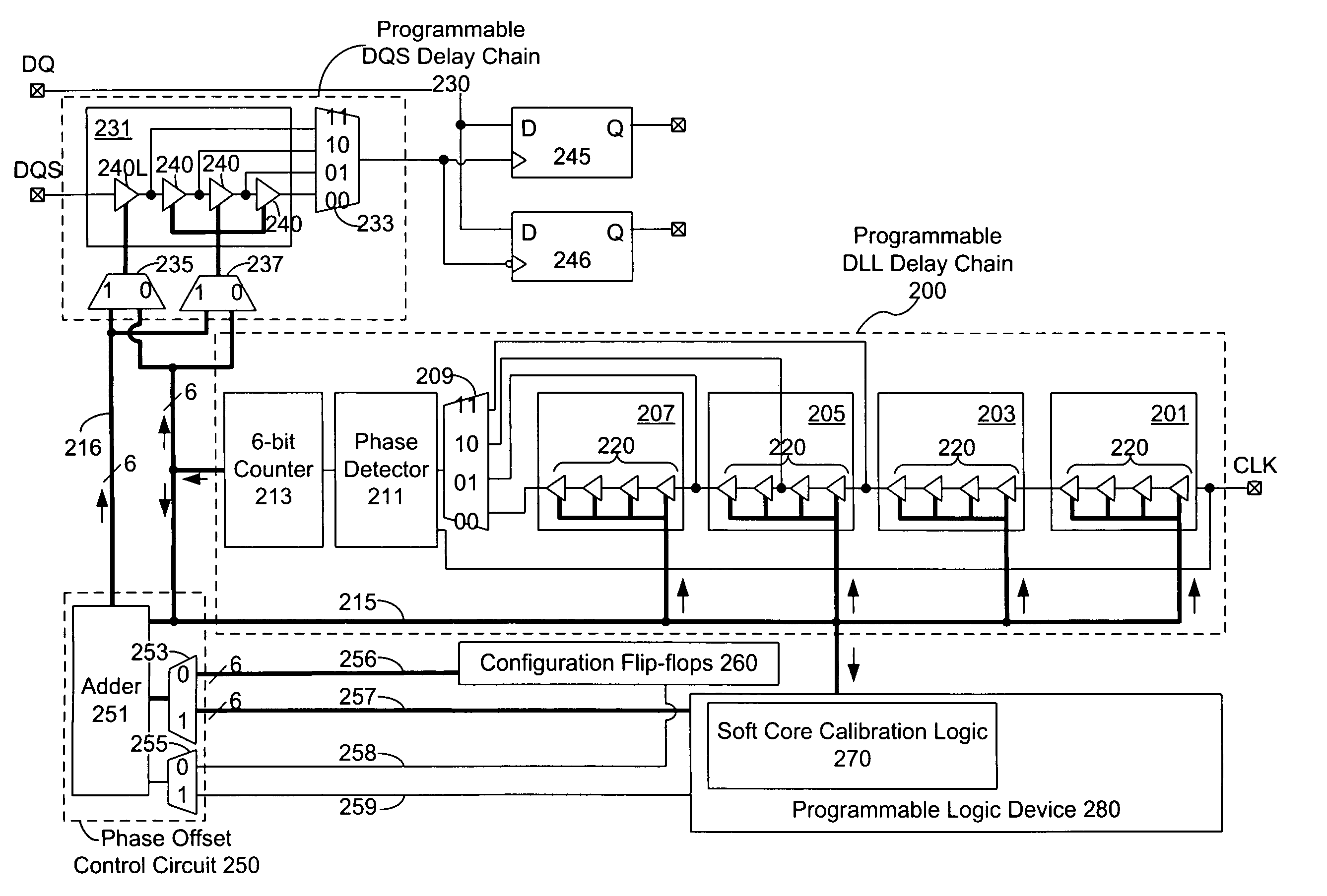
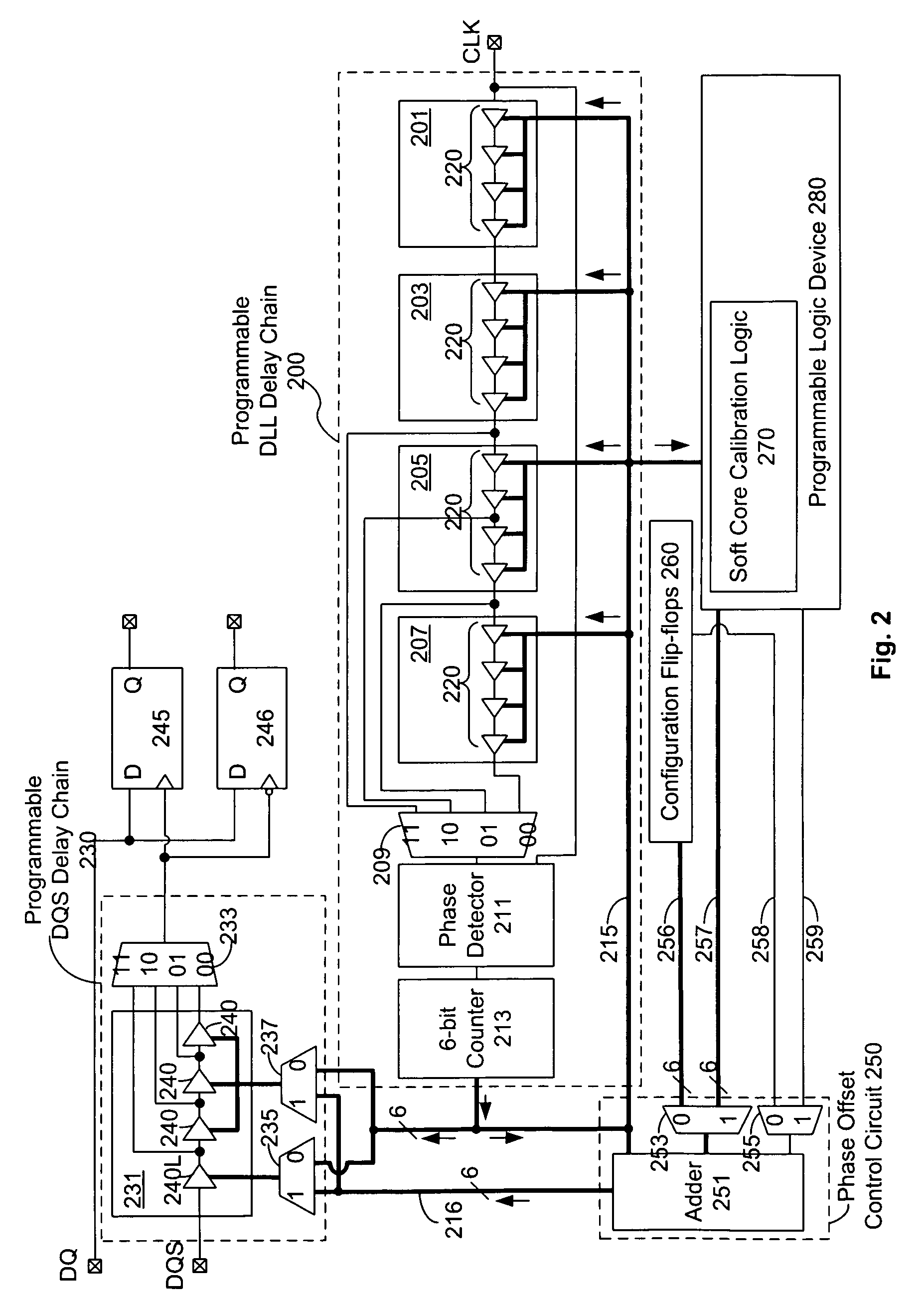
[0017]FIG. 2 is a diagram illustrative of a programmable memory interface circuit architecture according to one embodiment of the present invention. The interface circuit primarily includes three functionally distinct components, i.e., a programmable delay locked loop (DLL) delay chain 200, a phase offset control circuit 250 and a programmable DQS delay chain 230. A pair of DQ and DQS signals coming from a memory device (not shown) enters the interface circuit at respective DQ and DQS terminals at the top-left corner of FIG. 2. The DQS signal passes through the programmable DQS delay chain 230 and incurs a desired amount of phase delay. The phase-delayed DQS signal is then used to sample the DQ signal at the two latches 245 and 246 with its two opposite edges.
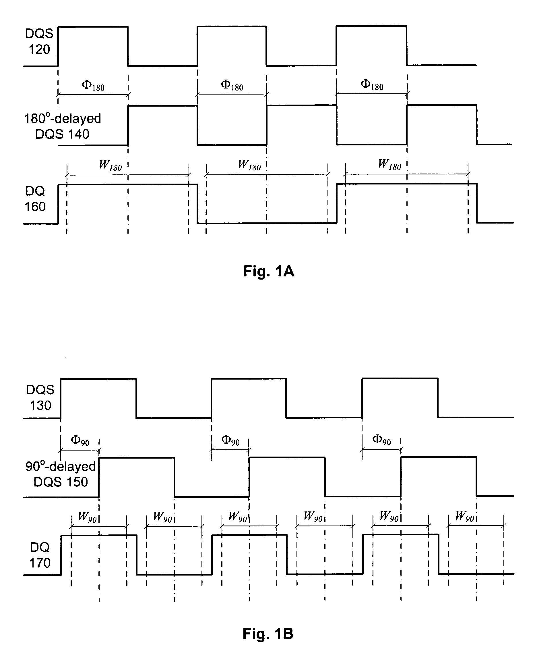
[0018]As discussed above, the phase delay applied to the DQS signal needs to be precise in order to shift the DQS signal's sampling edge exactly to the center of a data sampling window. The phase delay also needs to be dynamica...
PUM
 Abstract
Description
Claims
Application Information