Self-aligned double gate device and method for forming same

a double gate, self-aligning technology, applied in the direction of semiconductor devices, electrical devices, transistors, etc., can solve the problems of difficult to achieve the desired threshold voltage using conventional methods, complex and costly forming methods, and physical limitations of device behavior, so as to simplify the manufacturing process, improve the device performance, and increase the bottom gate voltage. effect of application

Inactive Publication Date: 2007-06-12
TAIWAN SEMICON MFG CO LTD
View PDF6 Cites 28 Cited by
  • Summary
  • Abstract
  • Description
  • Claims
  • Application Information

AI Technical Summary

Benefits of technology

[0009]The preferred embodiment of the present invention has a very thin buried insulating layer and thin channel. The thin buried oxide and thin channel not only improve the device performance, but also simplify the manufacturing process since the lower step height does not need to be filled. The preferred embodiment of the present invention integrates the process of forming the STI and the substrate contact by forming the substrate contact through the STI. The bottom gate voltage that can be applied is increased. Therefore the device performance is further improved.

Problems solved by technology

By this downscaling, the physical limitations of device behavior, as predicted for planar devices, are reached and partially exceeded.
The forming methods are complex and costly.
Channel thickness T is typically in the range of about 10 nm so that it is hard to use the conventional methods to achieve desired threshold voltage.
This significantly limits the performance improvement.
Typically, when high performance is desired, a higher bottom gate voltage can be applied so that the device has higher speed, although the sub-threshold leakage and power consumption are high.

Method used


Image

  • Self-aligned double gate device and method for forming same
  • Self-aligned double gate device and method for forming same
  • Self-aligned double gate device and method for forming same

Examples


Embodiment Construction

[0015]The making and using of the presently preferred embodiments are discussed in detail below. It should be appreciated, however, that the present invention provides many applicable inventive concepts that can be embodied in a wide variety of specific contexts. The specific embodiments discussed are merely illustrative of specific ways to make and use the invention, and do not limit the scope of the invention.

[0016]The cross sectional views of the intermediate stages of manufacturing preferred embodiments are illustrated in FIGS. 2 through 11, wherein like reference numbers are used to designate like elements throughout the various views and illustrative embodiments of the present invention.

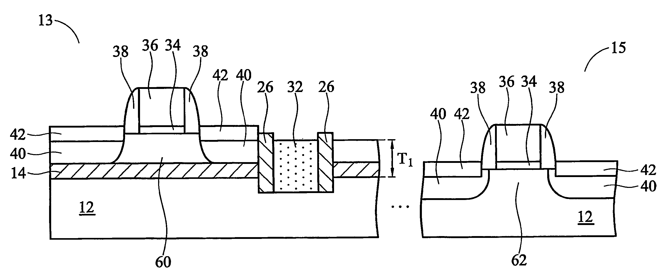
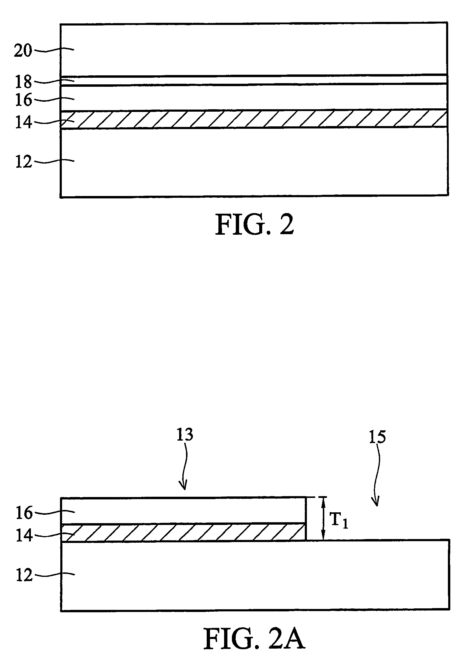
[0017]FIG. 2 illustrates a structure having a thin buried insulating layer, or preferably buried oxide (BOX) 14 and a second substrate 16 formed on a first substrate 12. The first substrate 12 is preferably a pre-doped silicon substrate. It can also be Ge, SieGe, SiGeC or the like. For NMOS dev...


PUM


Abstract

In a method of forming a double gate device, a buried insulating layer having a thickness of less than about 30 nm is formed on a first substrate. A second substrate is formed on the buried insulating layer. A pad layer is formed over the second substrate. A mask layer is formed over the pad layer. A first trench is formed extending through the pad layer, second substrate, buried insulating layer and into the first substrate. The first trench is filled with a first isolation. A second trench is formed in the first isolation and filled with a conductive material. An MOS transistor is formed on the second substrate. A bottom gate is formed under the buried insulating layer and self-aligned to the top gate formed on the second substrate.

Description

TECHNICAL FIELD[0001]This invention relates generally to semiconductor devices, and more specifically to the double gate MOS devices.BACKGROUND[0002]Double gate MOS devices have drawn increasing interest within the recent years because of their capability to reduce short channel effects. The downscaling of MOS devices will continue for the next decade. By this downscaling, the physical limitations of device behavior, as predicted for planar devices, are reached and partially exceeded. Thus, the so-called short channel effects become an issue, which is answered by the changing of device layout. For sub 50 nm devices, the double gate device layout is one of the most promising concepts to deal with the issue of short channel effects. Therefore, double gate devices have drawn increasing attention recent years. In double gate devices, there are two gates biased in parallel to form an inversion channel on both sides of a silicon layer. If the silicon layer is thin enough, these two invers...

Claims


Application Information

Patent Timeline
Patent Type & Authority Patents(United States)
IPC IPC(8): H01L29/10H01L27/01
CPCH01L27/1203H01L29/78648
Inventor CHEN, HAO-YUHSU, JU-WANGPERNG, BAW-CHINGYANG, FU-LIANG
Owner TAIWAN SEMICON MFG CO LTD
Why Eureka
Try Eureka