Plasma display panel having shared common electrodes mounted in areas corresponding to non-discharge regions

a technology of display panel and common electrode, which is applied in the direction of address electrode, static indicating device, instruments, etc., can solve the problems of uneven brightness over the screen of the pdp, mis-discharge of discharge cells adjacent along the direction of the address electrode, and low efficiency of energy conversion in each step, so as to prevent an increase in power consumption, enhance overall pdp efficiency, and maximize illumination efficiency

Inactive Publication Date: 2007-06-12
SAMSUNG SDI CO LTD
View PDF14 Cites 17 Cited by
  • Summary
  • Abstract
  • Description
  • Claims
  • Application Information

AI Technical Summary

Benefits of technology

[0017]In one exemplary embodiment of the present invention, there is provided a plasma display panel (PDP) that limits a discharge current in discharge cells to thereby prevent an increase in power consumption, and that maximizes illumination efficiency to enhance overall PDP efficiency.
[0018]Further, there is provided a PDP in which a pitch between discharge cells along a direction address electrodes are formed is reduced to thereby allow for more pixels to be formed and a higher picture quality to be obtained, and to thereby solve the problem of crosstalk between discharge cells along the direction of the address electrodes.

Problems solved by technology

However, the efficiency of energy conversion (i.e., brightness ratio relative to consumed power) in each of these steps is relatively low.
This results in a brightness over the screen of the PDP that is not uniform.
The second problem of the AC-PDP as indicated in the above-referenced application is that mis-discharge occurs between discharge cells adjacent along the direction the address electrodes are formed.
This may result in poor picture quality since unintended phosphor layers are illuminated.
However, there are significant drawbacks to such a structure disclosed in Japanese Laid-Open Patent No. 2000-285814.
This causes an increase in the amount of power consumed to thereby reduce PDP efficiency, and also acts as a hindrance to realizing uniform brightness in the discharge cells such that overall picture quality is reduced.
Another drawback to the above structure is that limitations are placed on increasing the number of pixels along the direction of the address electrodes by mounting three sustain electrodes for each discharge cell.
This limits attempts at enhancing picture quality.
However, with the above electrode structure and particularly the barrier rib structure described above, such a change in the discharge gas makes address discharge and sustain discharge unstable.
Therefore, only a very limited effectiveness of altering the discharge gas components is achieved.

Method used


Image

  • Plasma display panel having shared common electrodes mounted in areas corresponding to non-discharge regions
  • Plasma display panel having shared common electrodes mounted in areas corresponding to non-discharge regions
  • Plasma display panel having shared common electrodes mounted in areas corresponding to non-discharge regions

Examples


Embodiment Construction

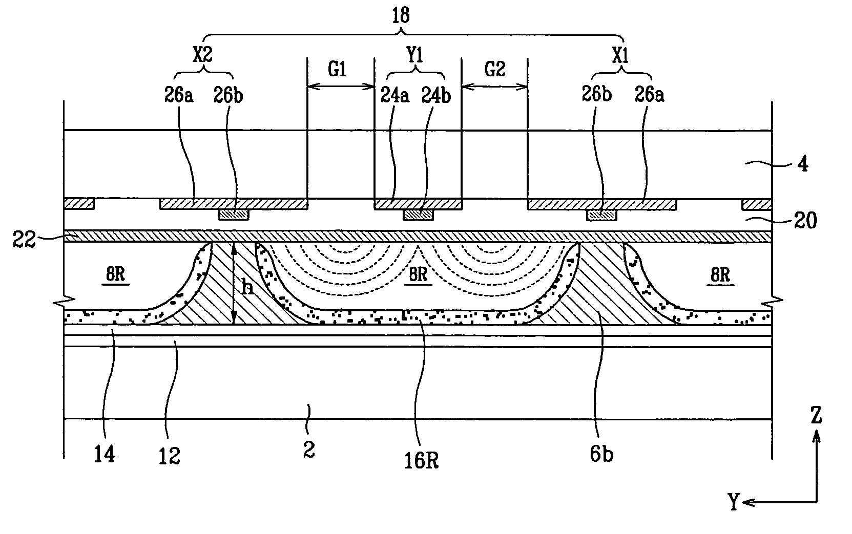
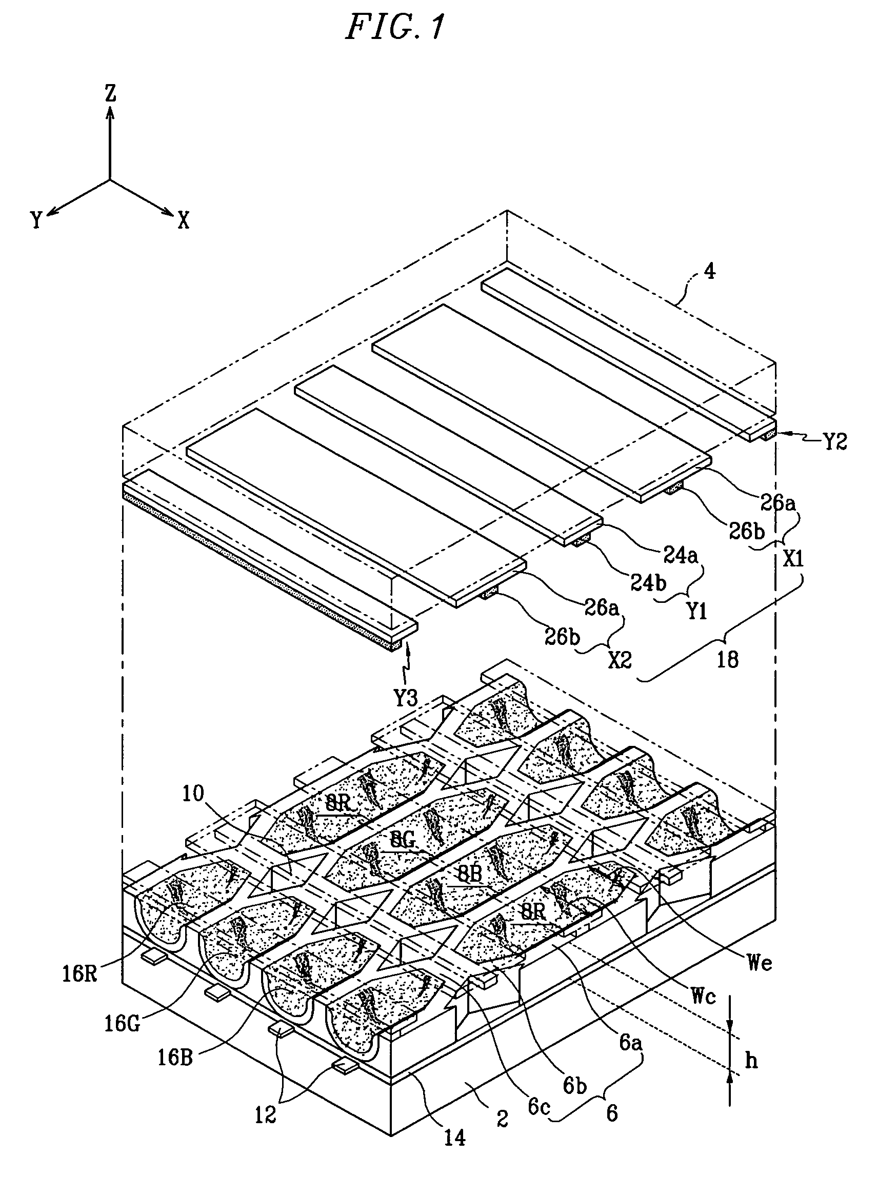
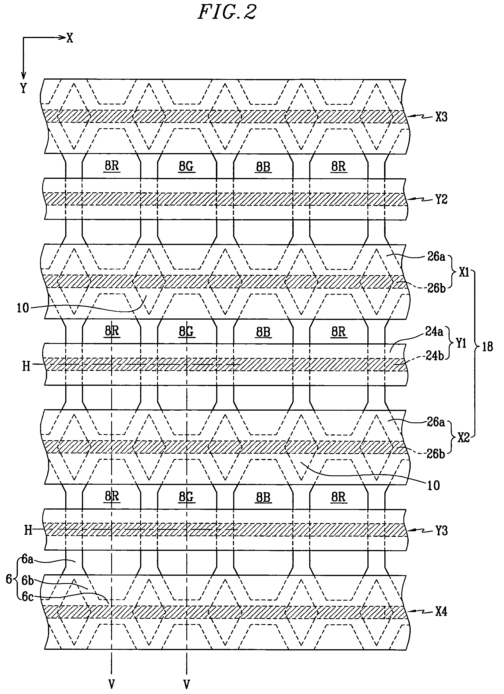
[0033]Referring to FIGS. 1 and 2, a PDP according to an exemplary embodiment of the present invention includes first substrate 2 and second substrate 4 provided opposing one another with a predetermined gap therebetween. Non-discharge regions 10 and discharge cells 8R, 8G, 8B are defined by barrier ribs 6 formed between first substrate 2 and second substrate 4. A discharge gas (an Ne—Xe compound gas) is filled in discharge cells 8R, 8G, 8B.

[0034]A plurality of address electrodes 12 is formed along one direction (direction Y in the drawings) on a surface of first substrate 2 opposing second substrate 4. As an example, address electrodes 12 are formed in a striped pattern with a uniform, predetermined interval between adjacent address electrodes 12. First dielectric layer 14 is formed over the entire surface of first substrate 2 covering address electrodes 12.

[0035]Barrier ribs 6 are mounted on first dielectric layer 14 to define non-discharge regions 10 and discharge cells 8R, 8G, 8B...


PUM


Abstract

A plasma display panel includes opposing first and second substrates provided with a predetermined gap therebetween. Address electrodes are formed on the first substrate. Barrier ribs are mounted in the gap between the first and second substrates to define discharge cells. Phosphor layers are formed within each discharge cell. Sustain electrodes are formed on the second substrate along a direction perpendicular to the address electrodes. The sustain electrodes include scan electrodes and common electrodes. One scan electrode is formed for each row of the discharge cells formed along the direction perpendicular to the address electrodes, and two common electrodes are formed for each such row of the discharge cells. Furthermore, each common electrode is shared among adjacent rows of the discharge cells. The common electrodes are mounted corresponding to non-discharge regions.

Description

CROSS-REFERENCE TO RELATED APPLICATIONS[0001]This application claims priority to and the benefit of Korean Patent Application No. 2003-0072363 filed on Oct. 16, 2003 in the Korean Intellectual Property Office, the entire content of which is incorporated herein by reference.BACKGROUND OF THE INVENTION[0002](a) Field of the Invention[0003]The present invention relates to a plasma display panel (PDP). More particularly, the present invention relates to an AC-PDP that forms discharge cells by including address electrodes on a rear substrate, and sustain electrodes comprised of scan electrodes and common electrodes on a front substrate.[0004](b) Description of the Related Art[0005]A PDP is a display device that uses vacuum ultraviolet rays generated by gas discharge in discharge cells to excite phosphors, thereby realizing the display of images. With its ability to realize high-resolution images, the PDP is emerging as one of the most popular flat panel display configurations used for wa...

Claims


Application Information

Patent Timeline
Patent Type & Authority Patents(United States)
IPC IPC(8): H01J17/49G09G3/10H01J11/12H01J11/22H01J11/24H01J11/26H01J11/32H01J11/34H01J11/36
CPCH01J11/12H01J11/32H01J2211/323H01J2211/326H01J2211/365H01J11/24H01J11/36
Inventor KWON, JAE-IKKANG, KYOUNG-DOO
Owner SAMSUNG SDI CO LTD
Why Eureka
Try Eureka