Integrated circuit with an electrostatic discharge protection circuit

a protection circuit and integrated circuit technology, applied in the direction of emergency protection arrangements for limiting excess voltage/current, etc., can solve the problem of different esd protection capabilities, triggering the voltage of the transistor b>34/b> in the breakdown situation, and providing a one-way esd protection circuit with lower esd protection capability

Inactive Publication Date: 2007-06-19
NOVATEK MICROELECTRONICS CORP
View PDF6 Cites 11 Cited by
  • Summary
  • Abstract
  • Description
  • Claims
  • Application Information

AI Technical Summary

Benefits of technology

[0014]The claimed invention provides an integrated circuit with an electrostatic discharge protection circuit. The integrated circuit comprises a first power pad, a second power pad, a power clamp circuit, an internal circuit, a signal pad, a bipolar junction transistor, and a metal-oxide semiconductor transistor. The power clamp circuit is electrically connected between the first power pad and the second power pad; the internal circuit is electrically connected between the first power pad and the second power pad; the signal pad is ele

Problems solved by technology

However, these components have different properties and thereby have different ESD protection capabilities.
Therefore, it only provides a one-way ESD protection circuit with lower ESD protection capability than that of FIG. 1.
However, the drawback is that the triggering voltage of the transistor 34 in the breakdown situation is high.

Method used


Image

  • Integrated circuit with an electrostatic discharge protection circuit
  • Integrated circuit with an electrostatic discharge protection circuit
  • Integrated circuit with an electrostatic discharge protection circuit

Examples


Embodiment Construction

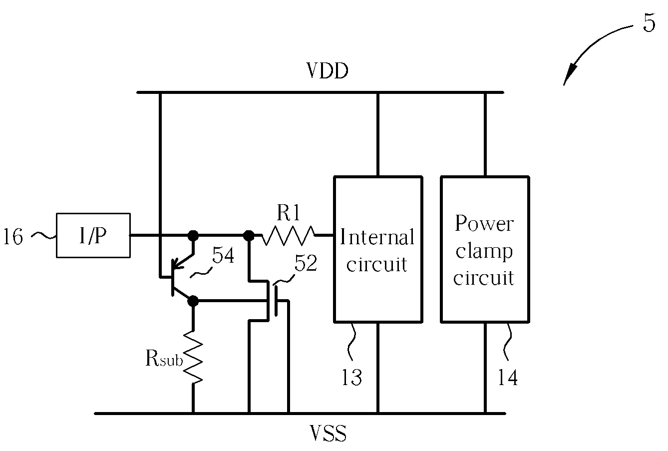
[0018]Please refer to FIGS. 5 and 6. FIG. 5 is a diagram of an input ESD protection circuit in an integrated circuit 5 based on the present invention. FIG. 6 is a diagram of an output ESD protection circuit in an integrated circuit 6 based on the present invention. The input ESD protection circuit of the IC 5 comprises an NMOS transistor 52 and a bipolar junction transistor 54 for ESD protection. The NMOS transistor 52 has a drain electrically connected to the input pad 16, a source and a gate both electrically connected to ground (VSS). The bipolar junction transistor 54 has a base electrically connected to VDD, an emitter electrically connected to the input pad 16, and a collector electrically connected to a body of the NMOS transistor 52. A parasitical resistance is between the collector of the bipolar junction transistor 54 and VSS.

[0019]The output stage of the IC 6 comprises an output pad (O / P) 17, an output resistor R4, an NMOS transistor 61, a PMOS transistor 63, two resistor...


PUM


Abstract

MOS Transistors and bipolar junction transistors are connected to input pads and output pads for implementing electrostatic discharge protection. By conducting a power clamp circuit and applying a substrate-trigger technology, electrostatic discharge protection is further enhanced. For instance, positive ESD stress protection can be enhanced between signal pads (input pads and output pads) and VSS by using NMOS transistors and field oxide devices. Negative ESD stress protection can be enhanced between signal pads and VDD by using PMOS transistors.

Description

BACKGROUND OF THE INVENTION[0001]1. Field of the Invention[0002]The present invention relates to an integrated circuit, and more particularly, to an integrated circuit with an electrostatic discharge protection circuit.[0003]2. Description of the Prior Art[0004]Generally, electrostatic discharge (ESD) stress testing for integrated circuits (ICs) include pin-to-pin testing modes, such as a positive-to-VSS (PS) mode, a negative-to-VSS (NS) mode, a positive-to-VDD (PD) mode and a negative-to-VDD (ND) mode, and a testing mode between power pins, such as a VDD-to-VSS (DS) mode. Take the PS mode for example. A positive ESD stress is applied to an input pin to be tested so as to discharge a VSS pin connected to ground while a VDD pin and other pins are floating.[0005]For complementary metal-oxide semiconductor (CMOS) integrated circuits, components for ESD protection circuits can be diffusion or poly-resistors, diodes with p-n junction, MOS transistors, field-oxide devices, bipolar junctio...

Claims


Application Information

Patent Timeline
IPC IPC(8): H02H3/22
CPCH01L27/0266
Inventor CHEN, SHIAO-SHIEN
Owner NOVATEK MICROELECTRONICS CORP
Why Eureka
Try Eureka