Stacked package structure

a technology of stacking and package structure, applied in the direction of semiconductor devices, semiconductor/solid-state device details, electrical equipment, etc., can solve the problems of substantial increase in cost, serious deterioration of stacking package structure, and greatly reduced yield of package process, so as to reduce the area occupied by the stacking package structure and reduce the area of the printed circuit board

Active Publication Date: 2007-07-10
ADVANCED SEMICON ENG INC
View PDF6 Cites 410 Cited by
  • Summary
  • Abstract
  • Description
  • Claims
  • Application Information

AI Technical Summary

Benefits of technology

[0007]Therefore, one objective of the present invention is to provide a stacked package structure, which ca

Problems solved by technology

As a result, the reliability of the stacked package structure is seriously deteriorated, th

Method used


Image

  • Stacked package structure
  • Stacked package structure
  • Stacked package structure

Examples


Embodiment Construction

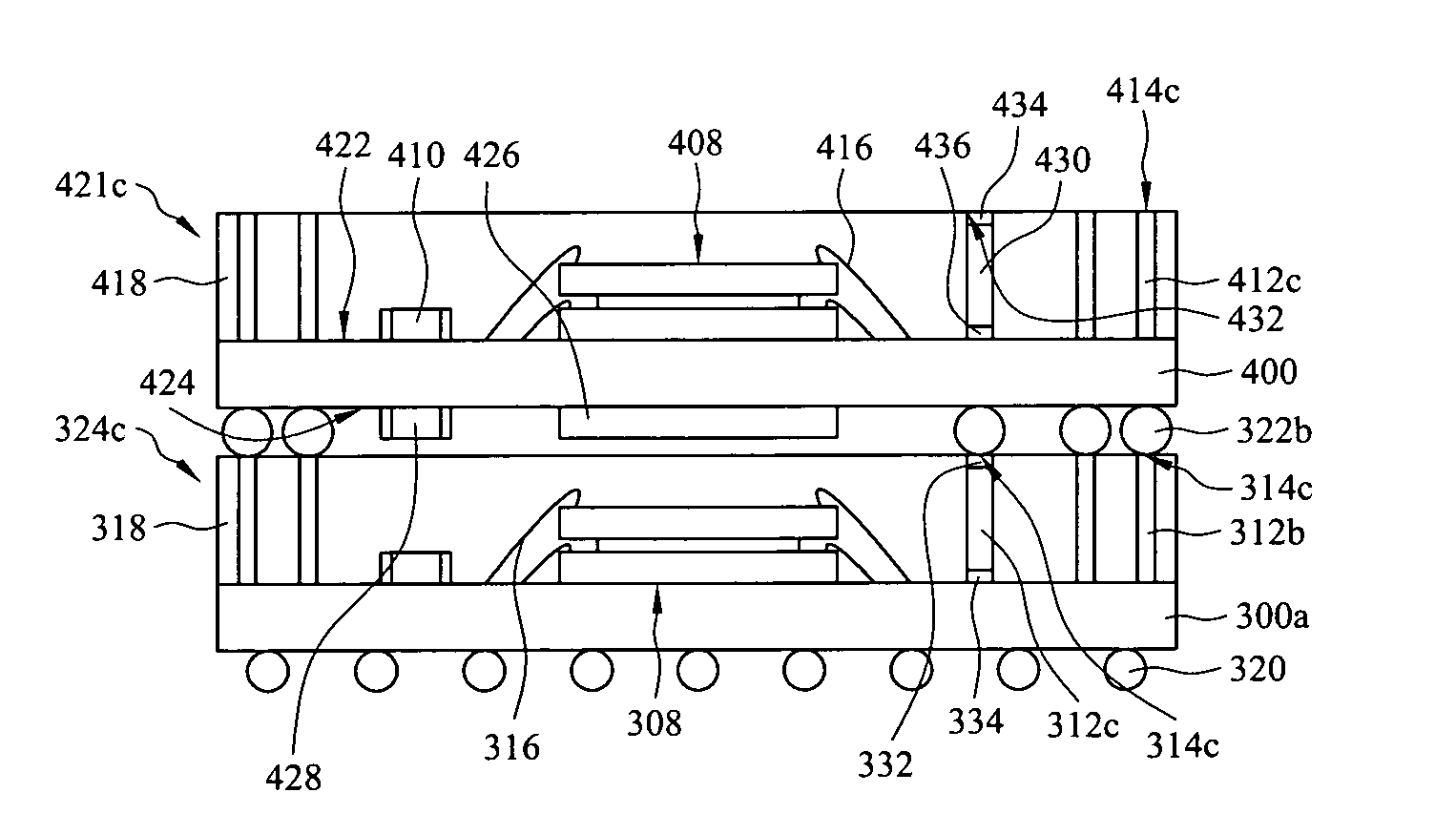
[0022]The present invention discloses a stacked package structure and a method for manufacturing the same. In order to make the illustration of the present invention more explicit and complete, the following description is stated with reference to FIGS. 4 to 12c.

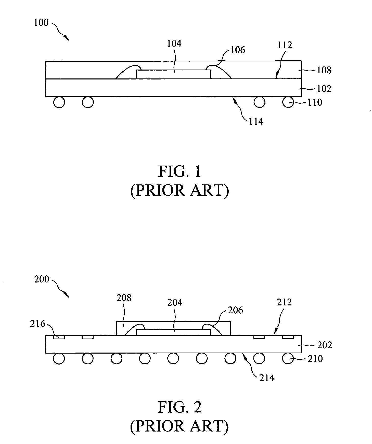
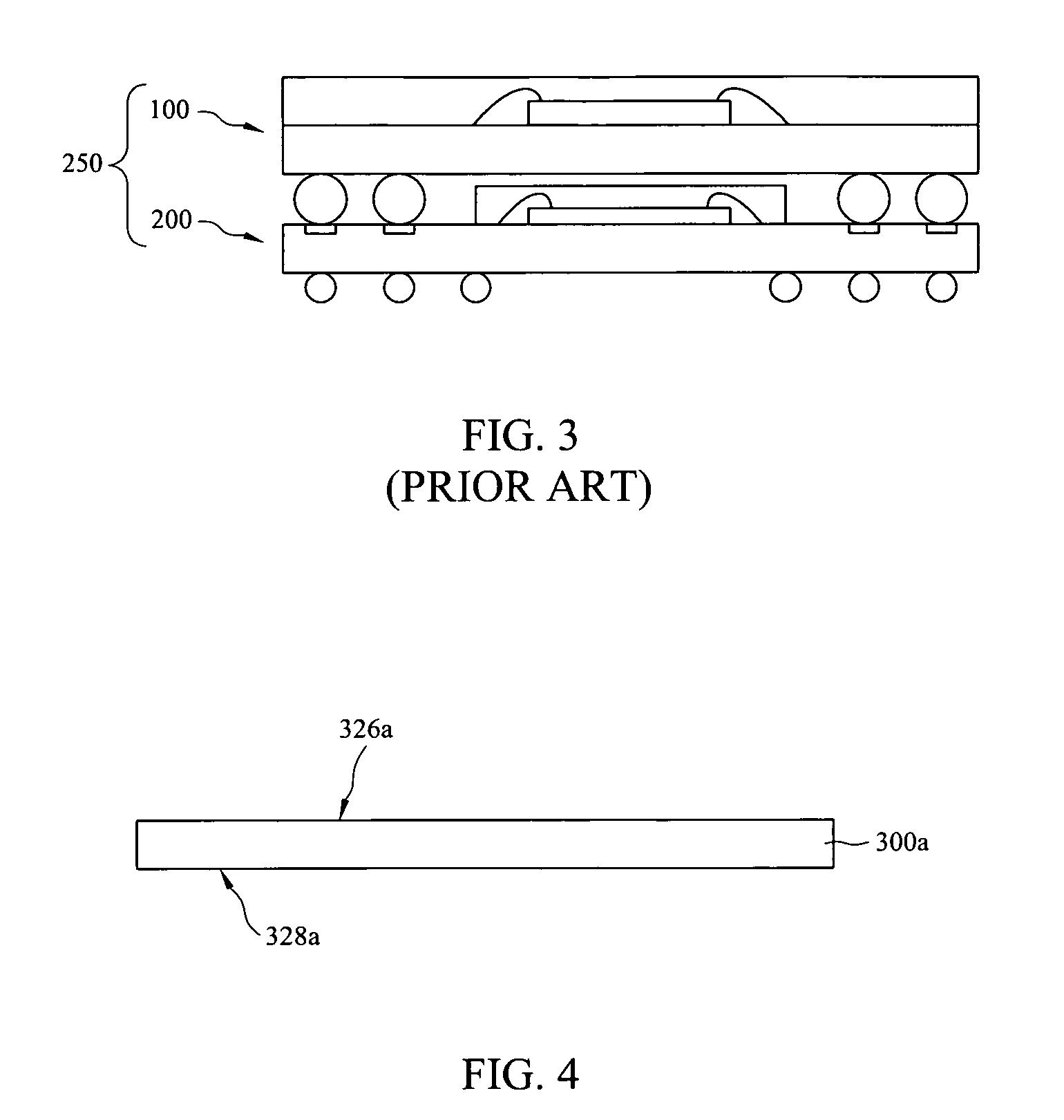
[0023]Referring to FIGS. 4 to 9b and FIG. 12a, in which FIGS. 4 to 9b are schematic flow diagrams showing the process for manufacturing a stacked package structure in accordance with a first preferred embodiment of the present invention. In the fabrication of a stacked package structure of the present invention, a chip package structure 324a, such as illustrated in FIG. 8, is typically formed firstly. In the formation of the chip package structure 324a, a substrate 300a or a substrate 300b is provided, in which the substrate 300a or the substrate 300b may be a printed circuit board, for example. The substrate 300a has a surface 326a and a surface 328a in opposition to each other, while the substrate 300b has a surface 326b ...


PUM


Abstract

A stacked package structure and a method for manufacturing the same are disclosed. The package structure comprises: a substrate having a first surface and a second surface in opposition to each other; at least one chip deposed on and electrically connected to the first surface of the substrate; a plurality of electrical connection devices deposed on the first surface and periphery of the substrate, wherein each electrical connection device is higher than the at least one chip in altitude; and an encapsulant covering the first surface of the substrate, the at least one chip and the electrical connection devices, wherein a top end of each electrical connection device is exposed at a surface of the encapsulant.

Description

FIELD OF THE INVENTION[0001]The present invention relates to a system-in-package (SiP) structure and a method for manufacturing the same, and more particularly, to a stacked package structure and a method for manufacturing the same.BACKGROUND OF THE INVENTION[0002]The demand for low cost, small size, and more functionality has become the main driving force in the electronic industry. To achieve such goals, advanced packaging techniques like flip chip, chip scale package, wafer level packaging, and 3D packages have been developed. The 3D packaging technique is developed to integrate dies, packages and passive components into one package, in other words, to achieve system in a package solution. The integration can be made in side-by-side, stacked, or both manners. The outstanding advantages of 3D package are small footprint, high performance and low cost.[0003]FIGS. 1 to 3 are schematic flow diagrams showing the process for manufacturing a conventional stacked package structure. In th...

Claims


Application Information

Patent Timeline
IPC IPC(8): H01L23/02
CPCH01L25/0657H01L25/105H01L25/16H01L2224/48091H01L2224/48227H01L2225/0651H01L2225/06589H01L2225/1052H01L2924/01078H01L2924/01079H01L2924/15311H01L2924/15331H01L2924/19041H01L2924/19105H01L2924/19106H01L2924/00014H01L2924/19107H01L2924/3511H01L2225/1023H01L2225/1058H01L2224/32145H01L2224/32225H01L2224/73265H01L2924/00012H01L2924/00H01L2924/181H01L24/73
Inventor LEE, YONGGILL
Owner ADVANCED SEMICON ENG INC
Why Eureka
Try Eureka