Probe card for semiconductor wafers having mounting plate and socket

Inactive Publication Date: 2007-07-31
MICRON TECH INC
View PDF58 Cites 5 Cited by
  • Summary
  • Abstract
  • Description
  • Claims
  • Application Information

AI Technical Summary

Benefits of technology

[0017]The probe card can also include a compressible member mounted to a surface (e.g., backside) of the interconnect substrate. The compressible member cushions the forces applied by the testing apparatus to the wafers, and allows the interconnect substrate to self planarize to the contact locations on the wafers. The compressible member can be formed of an elastomeric material, as a gas filled bladder, or as a sealed space for retaining compressed air. The compressible member can also be formed of a metal elastomer to provide heat conduction from the interconnect substrate and wafer.
[0018]In an illustrative embodiment of the probe card, the contact members comprise raised members having penetrating projections covered with conductive layers. The penetrating projections can be configured to penetrate the contact locations on the wafer to a self limiting penetratio

Problems solved by technology

One problem with this type of conventional probe card is that the planarity and positions of the needle probes can vary.
This is a very labor intensive procedure.
This can cause inaccuracies in the test results because electrical contact with the different contact locations can vary.
Continued use of the needle probes causes deformation and further misalignment of the needle probes.
Probe cards with needle probes are thus expensive to fabricate and expensive to maintain.
Another problem with needle probe cards is that the contact locations on the wafer are typically coated with a metal oxide layer.
This requires “overdrive” and “scrub” forces which can damage the contact locations and wafer.
Still another problem with needle probe cards is that they require the contact locations on the dice to be oversized.
One disadvantage of membrane probes is that vertical “overdrive” forces are required to penetrate the oxide and make a reliable electrical connection between the contact bumps on the probe and the contact locations on the wafer.
These forces can damage the contact locations and the wafer.
These forces can also cause the membrane to l

Method used


Image

  • Probe card for semiconductor wafers having mounting plate and socket
  • Probe card for semiconductor wafers having mounting plate and socket
  • Probe card for semiconductor wafers having mounting plate and socket

Examples


Example

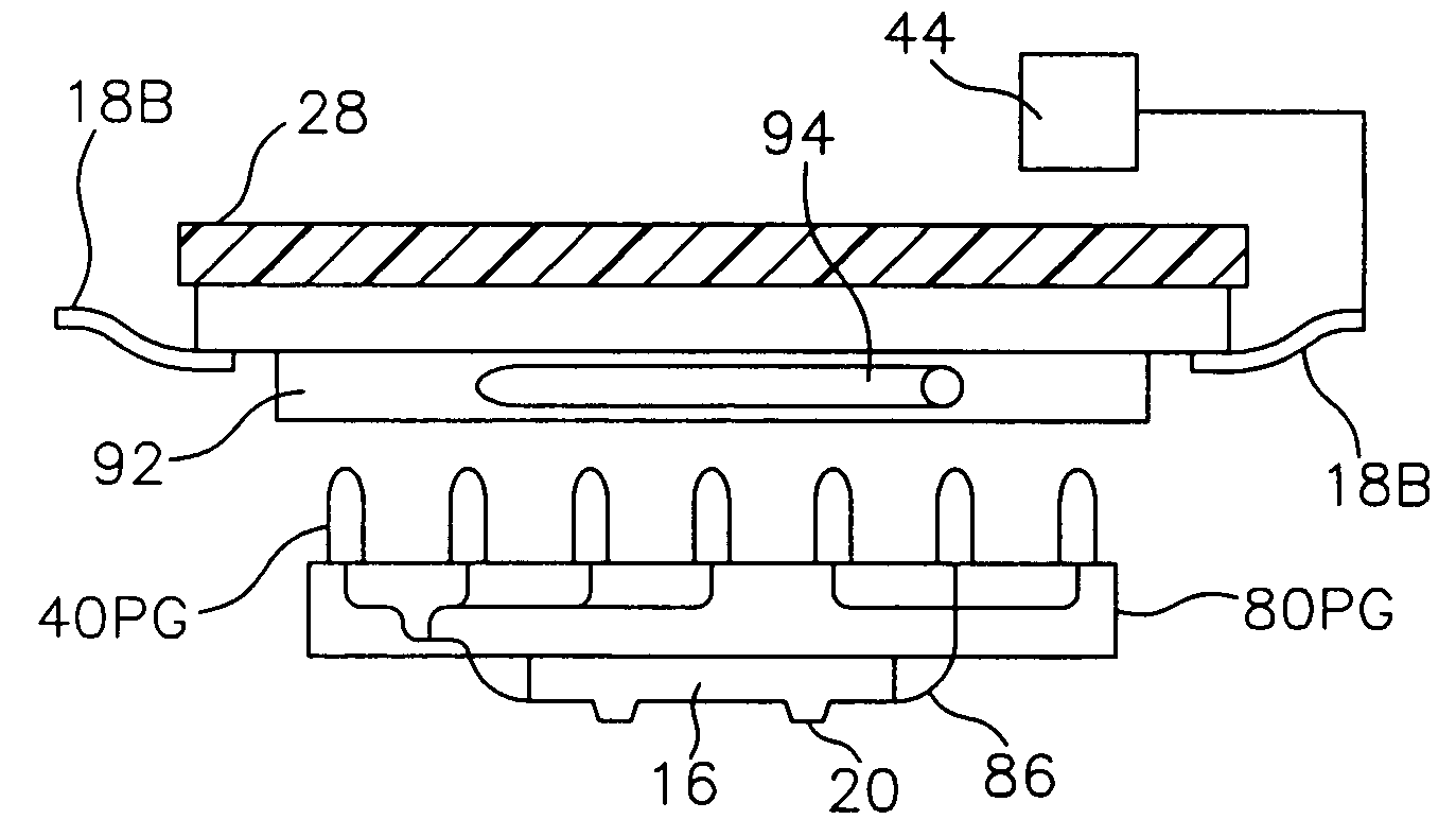
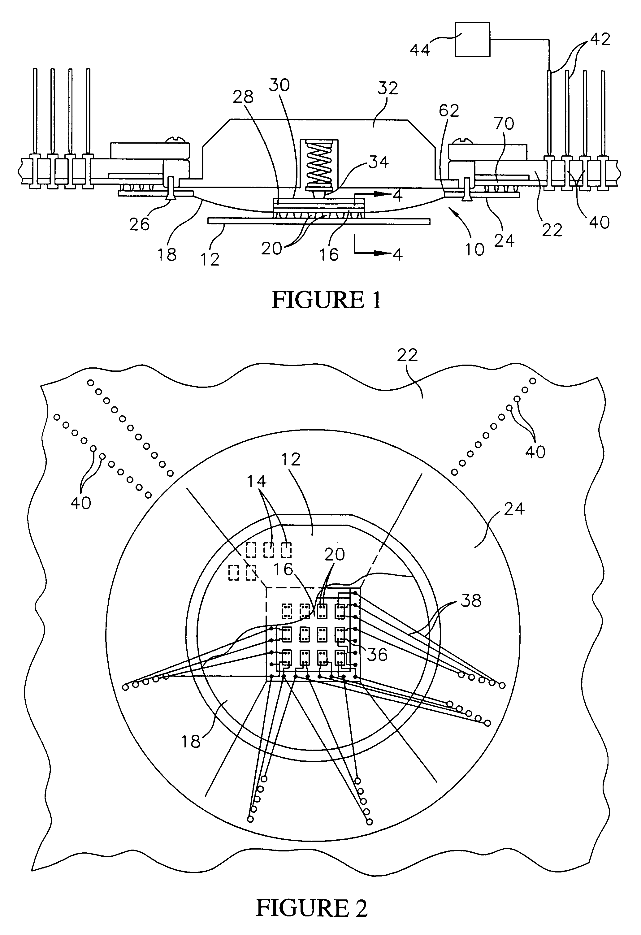
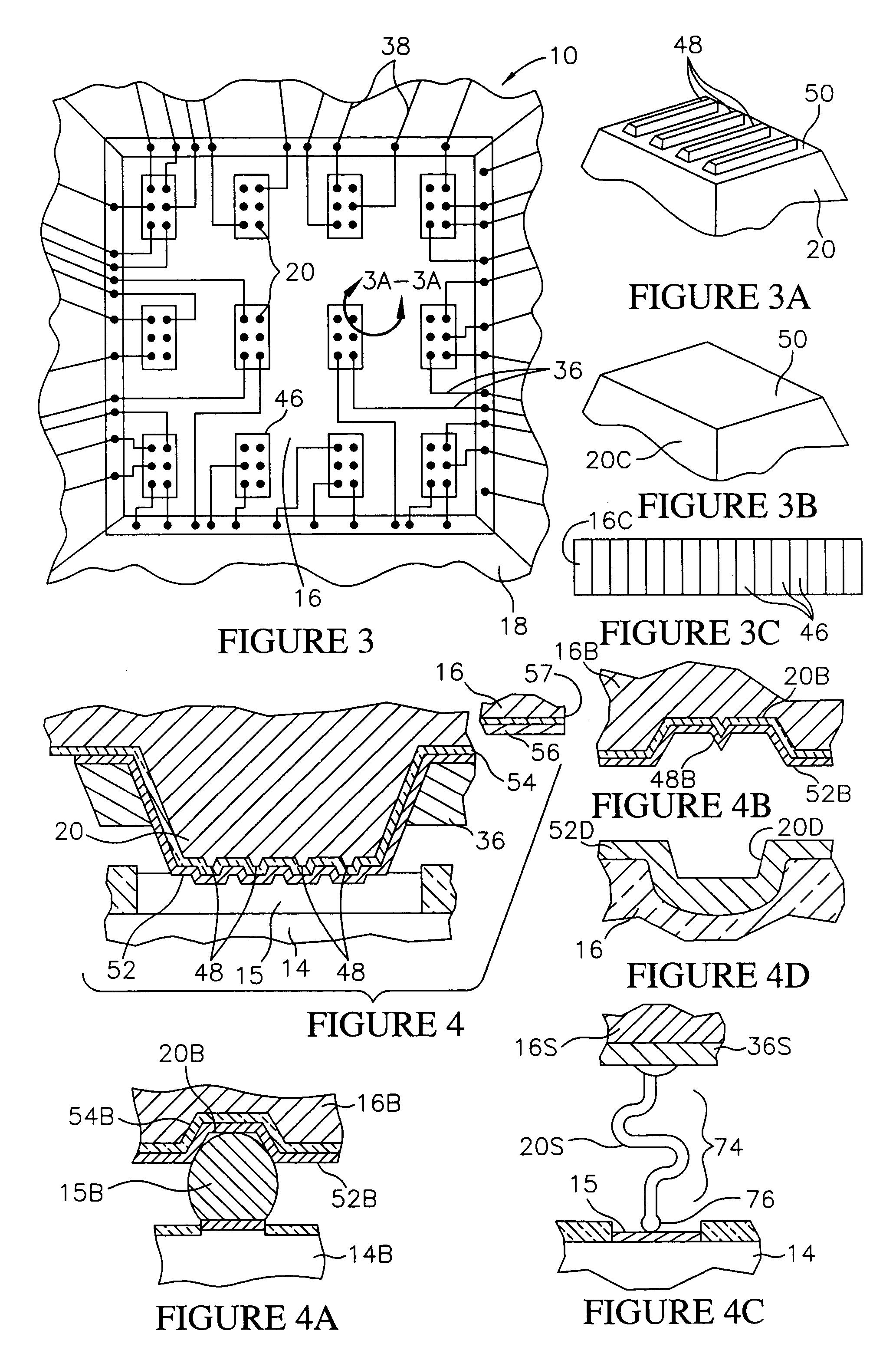
[0047]Referring to FIGS. 1 and 2, a probe card 10 constructed in accordance with the invention is shown during testing of a semiconductor wafer 12. The wafer 12 includes a plurality of semiconductor dice 14 (FIG. 2) each having a plurality of contact locations 15 (FIG. 4). The contact locations 15 are in electrical communication with the integrated circuits and semiconductor devices formed on the dice 14 and provide electrical access for testing.

[0048]In FIG. 1, the wafer 12 is supported circuit side up for contact with the probe card 10. The wafer 12 can be an entire semiconductor wafer 12 or portion of a wafer or other semiconducting substrate. A conventional testing apparatus such as a wafer probe handler (not shown) can be used to support and bias the probe card 10 and wafer 12 together during the testing procedure. The wafer probe handler can include a chuck (not shown) for supporting the wafer 12. Suitable wafer probe handlers are manufactured by Electroglass and others.

[0049]...


PUM


Abstract

A probe card for testing semiconductor wafers, and a method and system for testing wafers using the probe card are provided. The probe card is configured for use with a conventional testing apparatus, such as a wafer probe handler, in electrical communication with test circuitry. The probe card includes an interconnect substrate having contact members for establishing electrical communication with contact locations on the wafer. The probe card also includes a membrane for physically and electrically connecting the interconnect substrate to the testing apparatus, and a compressible member for cushioning the pressure exerted on the interconnect substrate by the testing apparatus. The interconnect substrate can be formed of silicon with raised contact members having penetrating projections. Alternately the contact members can be formed as indentations for testing bumped wafers. The membrane can be similar to multi layered TAB tape including metal foil conductors attached to a flexible, electrically-insulating, elastomeric tape. The probe card can be configured to contact all of the dice on the wafer at the same time, so that test signals can be electronically applied to selected dice as required.

Description

CROSS REFERENCE TO RELATED APPLICATIONS[0001]This application is a continuation of Ser. No. 10 / 072,734, filed Feb. 5, 2002, U.S. Pat. No. 6,798,224, which is a division of Ser. No. 09 / 929,388, filed Aug. 14, 2001, U.S. Pat. No. 6,359,456 B1, which is a division of Ser. No. 09 / 303,367 filed Apr. 30, 1999, U.S. Pat. No. 6,275,052, which is a division of Ser. No. 08 / 797,719, filed Feb. 11, 1997, U.S. Pat. No. 6,060,891.FIELD OF THE INVENTION[0002]This invention relates generally to semiconductor manufacture and specifically to a probe card for establishing temporary electrical communication with a substrate, such as a semiconductor wafer. This invention also relates to a method for fabricating the probe card, to a method for testing substrates using the probe card, and to a system for testing substrates that includes the probe card.BACKGROUND OF THE INVENTION[0003]During a semiconductor fabrication process semiconductor dice are formed on a wafer. The wafer includes a semiconducting su...

Claims


Application Information

Patent Timeline
IPC IPC(8): G01R1/073G01R31/28
CPCG01R31/2886
Inventor HEMBREE, DAVID R.FARNWORTH, WARREN M.AKRAM, SALMANWOOD, ALAN G.DOHERTY, C. PATRICKKRIVY, ANDREW J.
Owner MICRON TECH INC
Why Eureka
Try Eureka