High density memory module using stacked printed circuit boards

a memory module and printed circuit board technology, applied in the field of computer modules, can solve the problems of affecting the performance of components,

Active Publication Date: 2007-08-07
NETLIST INC
View PDF26 Cites 183 Cited by
  • Summary
  • Abstract
  • Description
  • Claims
  • Application Information

AI Technical Summary

Problems solved by technology

Stacking configurations can cause problems due to power dissipation in the components which are in close proximity.
Some or all of the components can generate significant amounts of heat, which can raise the temperature of the component itself or of the surrounding components of the module.
The raised temperature of these components can have harmful effects on the performance of the components, causing them to malfunction.
However, the narrow air gap between the stacked PCBs would allow very little cool air from the ventilation fan to cool the components on the inside surfaces to within the specified operating temperatures.

Method used


Image

  • High density memory module using stacked printed circuit boards
  • High density memory module using stacked printed circuit boards
  • High density memory module using stacked printed circuit boards

Examples


Embodiment Construction

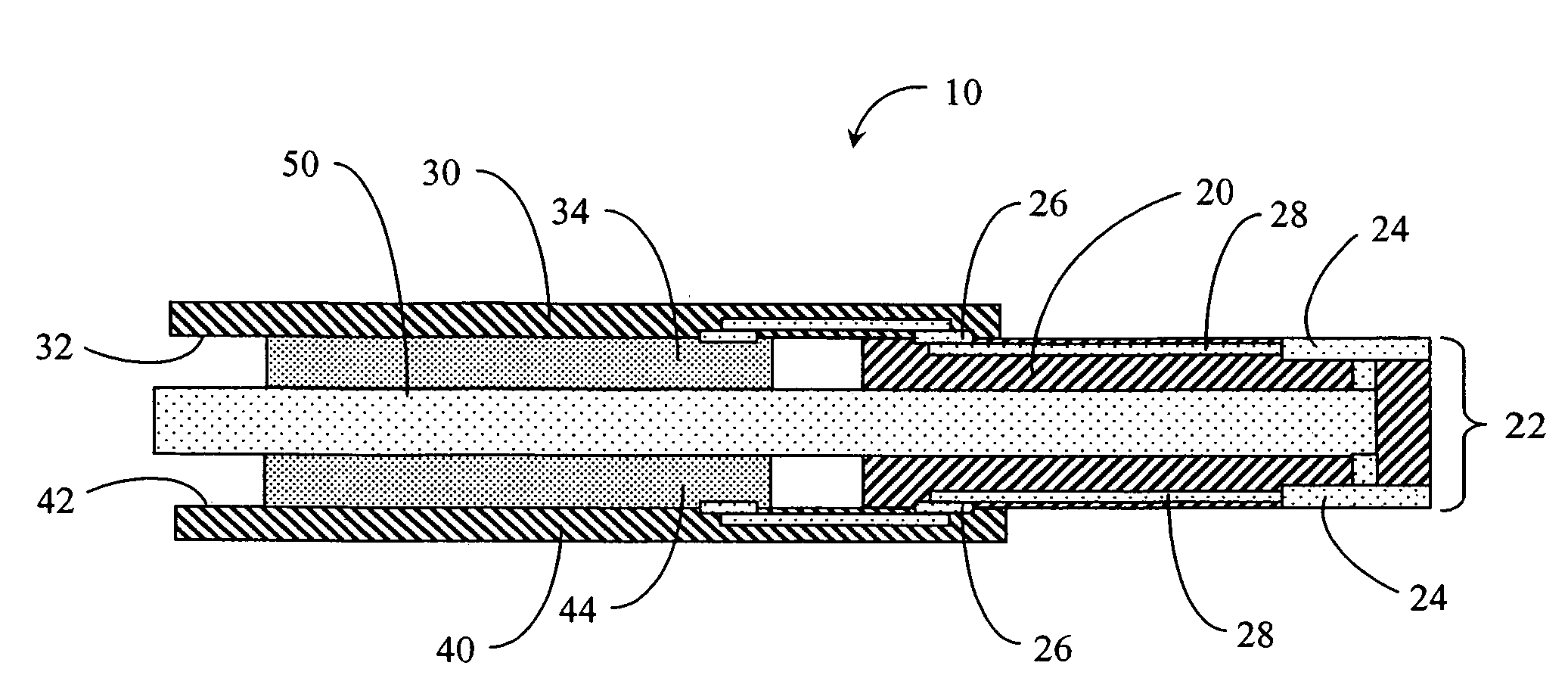
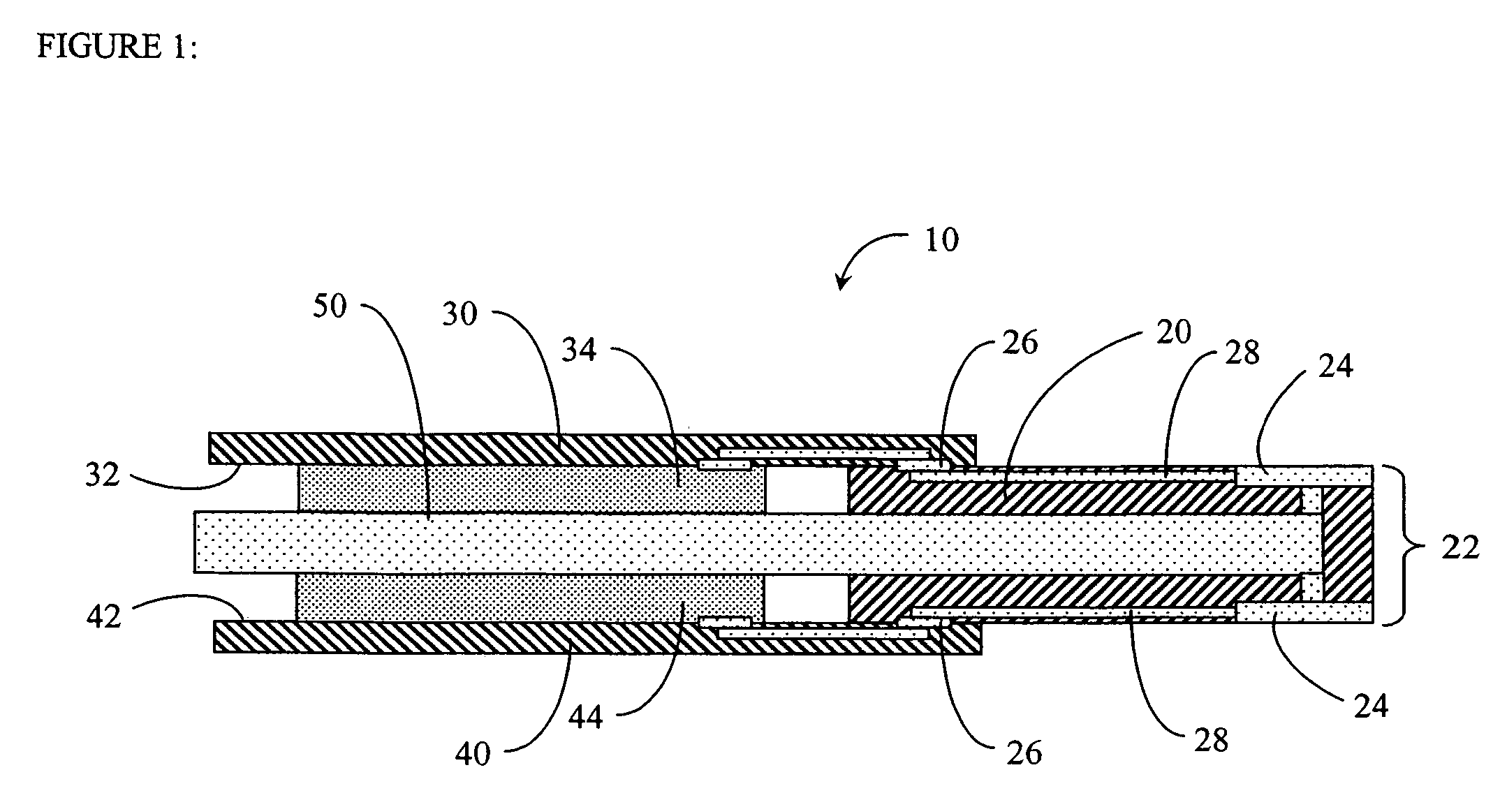
[0028]FIG. 1 schematically illustrates a cross-sectional view of a module 10 in accordance with certain embodiments described herein. The module 10 comprises a frame 20 having an edge connector 22 with a plurality of electrical contacts 24 which are electrically connectable to a computer system (not shown). The module 10 further comprises a first printed circuit board (PCB) 30 coupled to the frame 20. The first PCB 30 has a first surface 32 and a first plurality of components 34 mounted on the first surface 32 and electrically coupled to the electrical contacts 24 of the edge connector 22. The module 10 further comprises a second PCB 40 coupled to the frame 20. The second PCB 40 has a second surface 42 and a second plurality of components 44 mounted on the second surface 42 and electrically coupled to the electrical contacts 24 of the edge connector 22. The second surface 42 of the second PCB 40 faces the first surface 32 of the first PCB 30. The module 10 further comprises at least...


PUM

PropertyMeasurementUnit
thicknessaaaaaaaaaa
thicknessaaaaaaaaaa
electricallyaaaaaaaaaa

Abstract

A module is electrically connectable to a computer system. The module includes a frame having an edge connector with a plurality of electrical contacts which are electrically connectable to the computer system. The module further includes a first printed circuit board coupled to the frame. The first printed circuit board has a first surface and a first plurality of components mounted on the first surface. The first plurality of components is electrically coupled to the electrical contacts of the edge connector. The module further includes a second printed circuit board coupled to the frame. The second printed circuit board has a second surface and a second plurality of components mounted on the second surface. The second plurality of components is electrically coupled to the electrical contacts of the edge connector. The second surface of the second printed circuit board faces the first surface of the first printed circuit board. The module further includes at least one thermally conductive layer positioned between the first plurality of components and the second plurality of components. The at least one thermally conductive layer is thermally coupled to the first plurality of components, to the second plurality of components, and to the electrical contacts of the edge connector.

Description

CLAIM OF PRIORITY[0001]The present application claims the benefit of U.S. Provisional Application No. 60 / 561,009, filed Apr. 9, 2004, and U.S. Provisional Application No. 60 / 589,777, filed Jul. 21, 2004, each of which is incorporated in its entirety by reference herein.BACKGROUND OF THE INVENTION[0002]1. Field of the Invention[0003]The present invention relates generally to computer modules having a plurality of components mounted on two or more stacked printed circuit boards, and more specifically to high density memory modules using stacked printed circuit boards with heat dissipation structures.[0004]2. Description of the Related Art[0005]Computer systems often utilize modules comprising one or more printed circuit boards (PCBs). Each PCB has one or more components (e.g., integrated circuits or ICs) mounted thereon, and the components can be mounted on one side or on both sides of the PCB. In certain computer systems, the PCBs of the module are stacked next to one another to incr...

Claims


Application Information

Patent Timeline
Patent Type & Authority Patents(United States)
IPC IPC(8): H05K7/20
CPCH05K1/0203H05K1/144H05K2201/10189Y10T29/4913H05K2201/2018Y10T29/49124Y10T29/49117H05K2201/1056
Inventor PAULEY, ROBERT S.BHAKTA, JAYESH R.GERVASI, WILLIAM M.CHEN, CHI SHEDELVALLE, JOSE
Owner NETLIST INC
Why Eureka
Try Eureka