

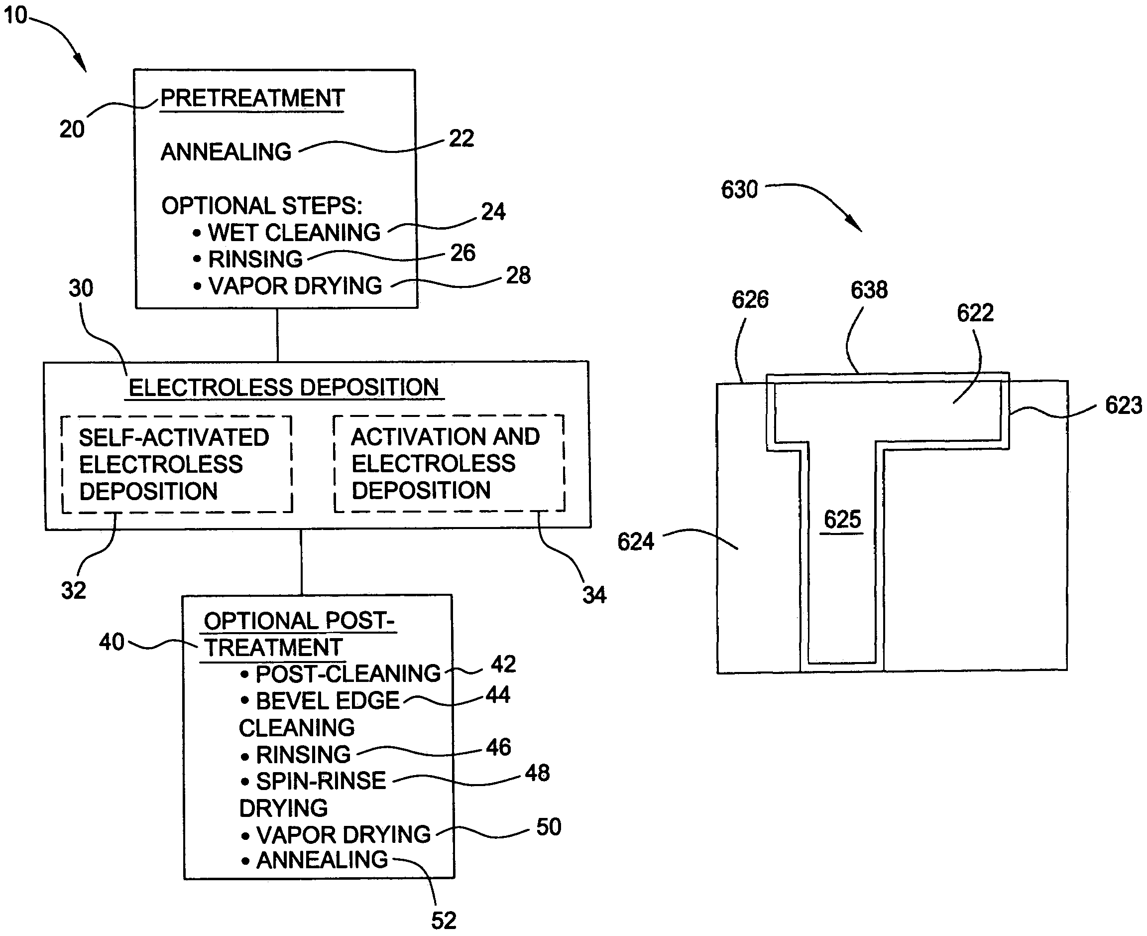
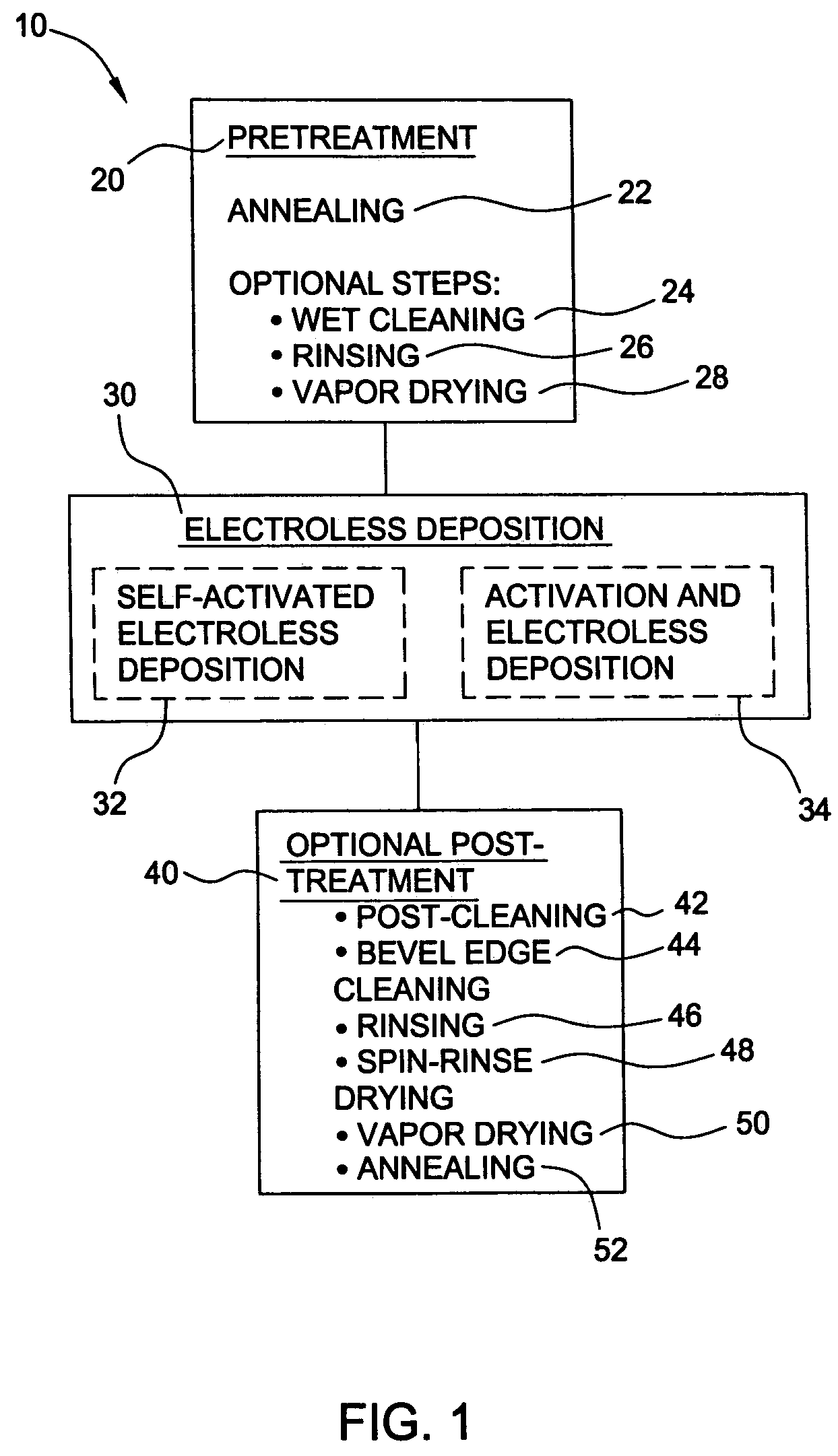
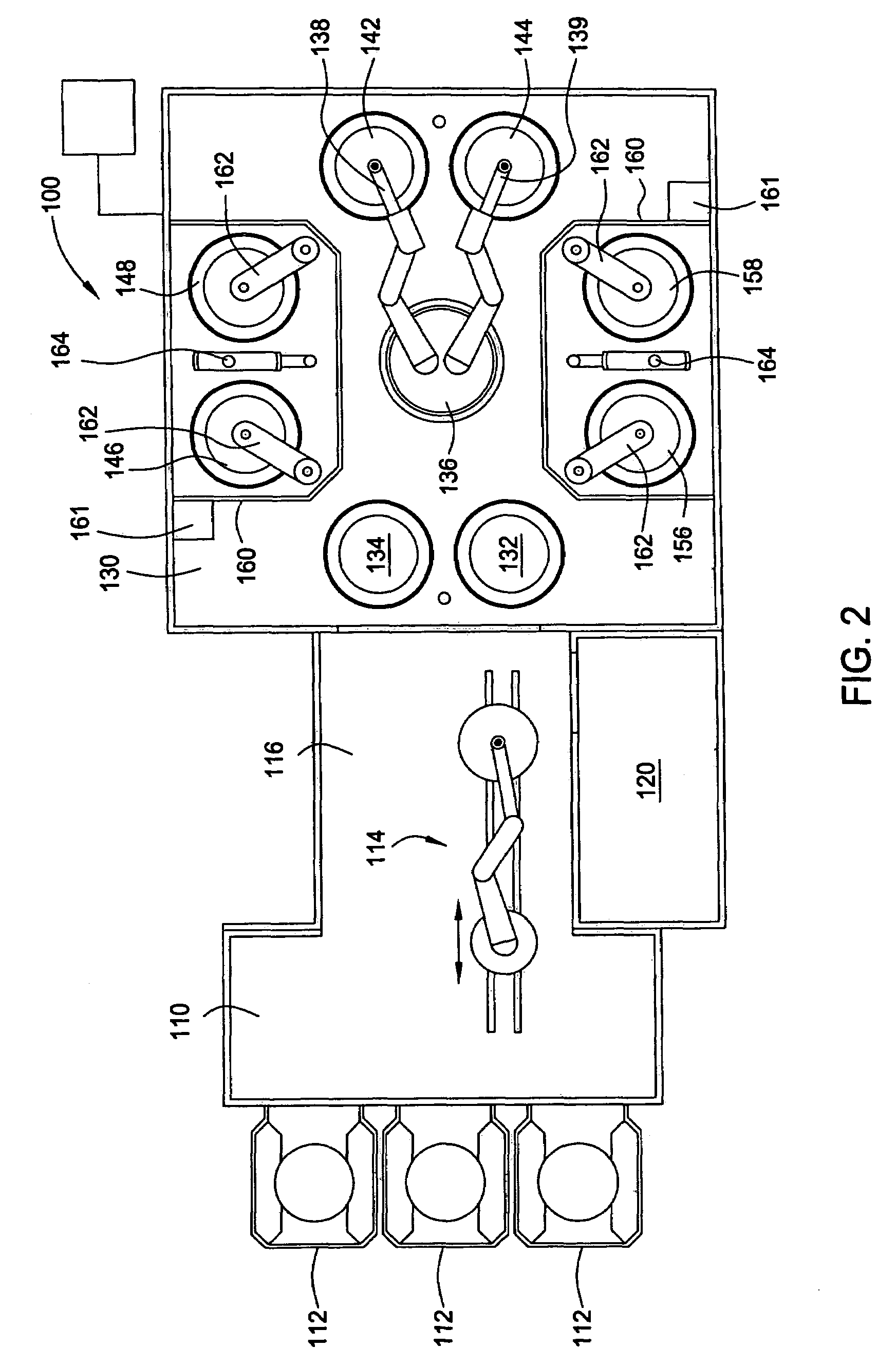
Pretreatment for electroless deposition
a technology of electroless deposition and pretreatment, which is applied in the direction of basic electric elements, electrical equipment, semiconductor/solid-state device manufacturing, etc., can solve the problems of sub-micron, sub-micron, and many traditional deposition processes that have difficulty in filling sub-micron structures, and the prior electroless deposition processing apparatus and method has faced substantial challenges in accurately controlling the electroless deposition process
- Summary
- Abstract
- Description
- Claims
- Application Information
AI Technical Summary
Benefits of technology
Problems solved by technology
Method used
Image

Examples
examples
[0047]Planarized semiconductor substrates comprising a dielectric layer having copper features formed therein were provided. For a first sample of substrates, a thermal anneal was performed at a temperature of about 350° C. in a reduced pressure environment with a gas mixture provided in a ratio of about 96:4 (v / v) noble gas to hydrogen gas. Then, an electroless deposition was performed over the pretreated substrates to form a cobalt comprising cap selectively over the copper features. For a second sample of substrates, a fluid was provided to pretreat the substrates. Then, electroless deposition was performed over the substrates to form a cobalt comprising cap selectively over the copper features. In a third sample of substrates, an electroless deposition was performed over the substrates to form a cobalt comprising cap selectively over the copper features without a fluid pretreatment or a thermal anneal pretreatment. Electrical tests showed improved leakage current results of the ...
PUM
| Property | Measurement | Unit |
|---|---|---|
| temperature | aaaaa | aaaaa |
| temperature | aaaaa | aaaaa |
| temperature | aaaaa | aaaaa |
Abstract
Description
Claims
Application Information